Supercharge Your Innovation With Domain-Expert AI Agents!

Multilayer Wiring Board and Its Manufacturing Method

a manufacturing method and multi-layer technology, applied in the direction of printed circuit manufacturing, printed circuit aspects, conductive pattern formation, etc., can solve the problems of inability to expect the compressing effect of conductive paste by burying the wiring into the electrical insulating substrate, thin multi-layer wiring board, and little compression property

Inactive Publication Date: 2008-12-18
PANASONIC CORP
View PDF4 Cites 3 Cited by
  • Summary
  • Abstract
  • Description
  • Claims
  • Application Information

AI Technical Summary

Benefits of technology

[0027]The present invention provides a multilayer wiring board employing a thin insulating substrate having only resin flow as compression property effect. The multilayer wiring board has an any-layer IVH (inner via hole) structure where at least one insulating substrate is formed without burying a wiring. Thus, crush-allowance of a conductor can be secured sufficiently, by increasing a ratio of a thickness of a cover film to that of the electrical insulating substrate. The conductor filled into via holes formed in the thin insulating substrate where the compression property effect can be hardly expected can be effectively compressed. As a result, a thin multilayer wiring board having an any-layer IVH structure and its manufacturing method can be provided.

Problems solved by technology

However, recently, it has been strongly demanded that the multilayer wiring board is thinned, and, when a thin electrical insulating substrate is employed for satisfying this demand, little compression property is demonstrated.
Therefore, the compressing effect of the conductive paste by burying the wiring into the electrical insulating substrate cannot be expected.
In other words, the conventional manufacturing method has the following problems when a multilayer wiring board having an any-layer IVH structure is manufactured using thin electrical insulating substrates.
As one problem, it is difficult to effectively compress the conductive paste and hence the electric connection resistance between the wiring material and the conductive paste varies on the high side.
As another problem, via resistance stability deteriorates in the reliability test.
Therefore, it is difficult to thin the multilayer wiring board having an any-layer IVH structure.

Method used


Image

  • Multilayer Wiring Board and Its Manufacturing Method
  • Multilayer Wiring Board and Its Manufacturing Method
  • Multilayer Wiring Board and Its Manufacturing Method

Examples


exemplary embodiment 1

[0073]Exemplary embodiment 1 of the present invention will be hereinafter described with reference to the drawings.

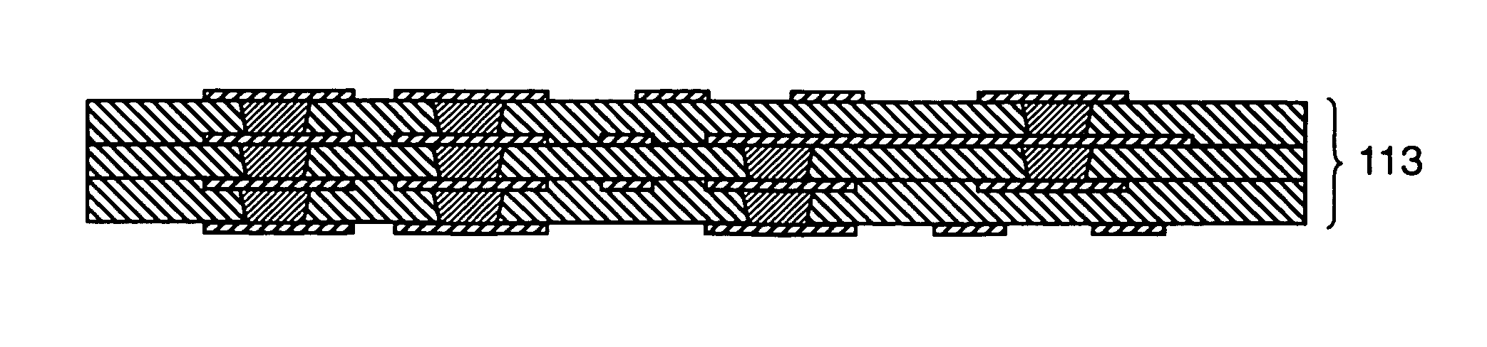
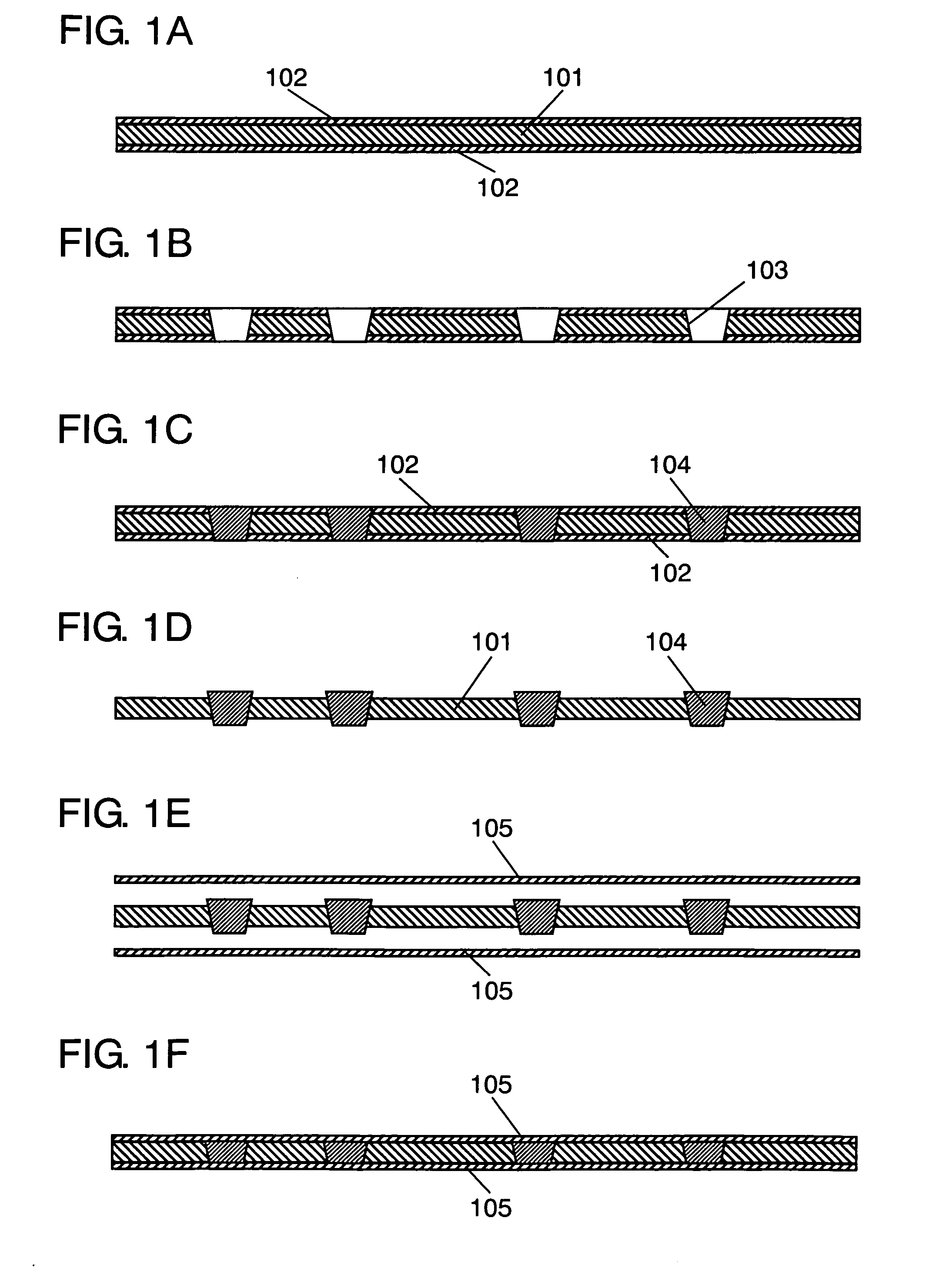
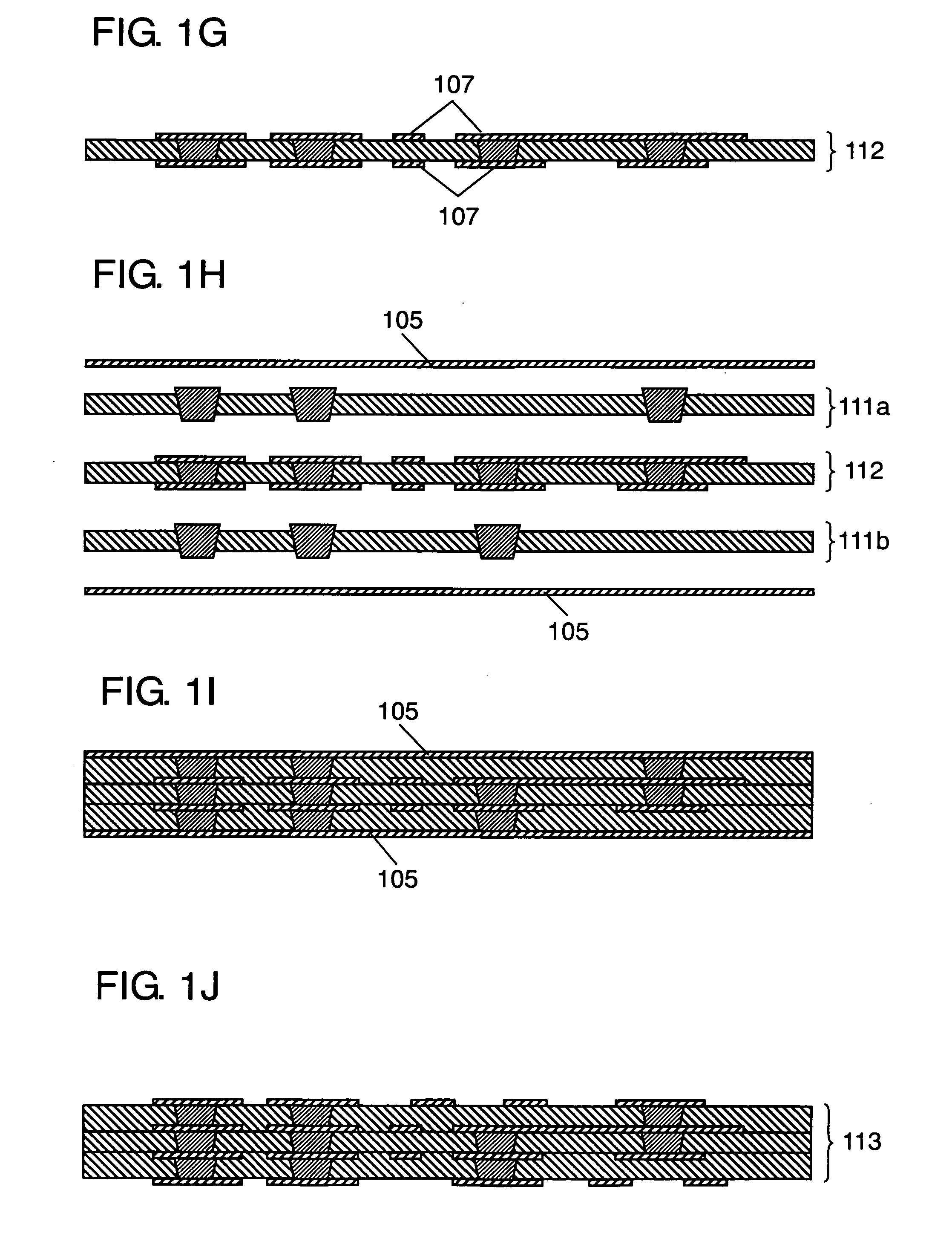
[0074]FIG. 1A through FIG. 1J are sectional views showing the steps of a manufacturing method of a multilayer wiring board in accordance with exemplary embodiment 1 of the present invention.

[0075]First, in FIG. 1A, cover films 102 are stuck to both sides of electrical insulating substrate 101.

[0076]Electrical insulating substrate 101 has substrate compressibility in a thickness direction of 5% or lower. As electrical insulating substrate 101, a composite substrate of porous substrate and resin, a substrate made of only thermosetting resin, or a composite substrate of fiber and resin is used. As the composite substrate of porous substrate and resin, a composite substrate formed by impregnating a porous film formed of extended PTFE (polytetrafluoroethylene) with epoxy resin and cyanate resin may be used. The single thermosetting resin is generally coated with epoxy resin....

exemplary embodiment 2

[0101]Exemplary embodiment 2 of the present invention will be hereinafter described with reference to the drawings.

[0102]FIG. 2A through FIG. 2J are sectional views showing the steps of a manufacturing method of a multilayer wiring board in accordance with exemplary embodiment 2 of the present invention. The descriptions of elements similar to those in embodiment 1 are simplified.

[0103]First, in FIG. 2A, electrical insulating adhesive 202 is applied to both surfaces of electrical insulating substrate 201, and cover films 203 are further stuck to both sides of the product.

[0104]Electrical insulating substrate 201 of FIG. 2A has substrate compressibility in the thickness direction of 5% or lower. Electrical insulating substrate 201 of the present embodiment is made of heat-resistant film material. For using the film material in a printed wiring board, preferably, the film material does not dissolve or soften even when it is heated to a reflow temperature, namely about 280° C. Material...


PUM

PropertyMeasurementUnit
Fractionaaaaaaaaaa
Fractionaaaaaaaaaa
Thicknessaaaaaaaaaa

Abstract

A multilayer wiring board employs a thin insulating substrate having substantially only resin flow as the compression property effect, and has an any-layer IVH structure where at least one core layer is formed without burying wiring. For sufficiently securing an effective compression amount of the crush-allowance of a conductor, the ratio of the thickness of a cover film to that of the electrical insulating substrate is increased, and a via can be formed in the core layer without burying the wiring in the insulating substrate. Thus, a multilayer wiring board having an any-layer IVH structure that can achieve high-density component mountability and wiring storability in an extremely small thickness can be provided.

Description

TECHNICAL FIELD[0001]The present invention relates to a manufacturing method of a multilayer wiring board, which has an especially thin any-layer inner via hole (IVH) structure, where vias for electrically interconnecting wiring layers of the multilayer wiring board and lands formed in the wiring layers are accurately positioned.BACKGROUND ART[0002]Recently, with decrease in size and increase in performance of electronic apparatuses, it has been strongly demanded that multilayer wiring boards on which semiconductor chips of large scale integration (LSI) or the like can be mounted in a high density are supplied inexpensively in a large field of not only industrial application but also consumer application. In such a multilayer wiring board, wiring patterns of a plurality of layers formed in a fine wiring pitch must be interconnected electrically with high wiring reliability, and the thinning of the board is strongly demanded.[0003]One conventional example satisfying such demands of t...

Claims


Application Information

Patent Timeline
IPC IPC(8): H05K1/05H05K3/10
CPCH05K3/4652H05K3/4655H05K2201/0355H05K2201/10378Y10T29/49155H05K2203/1461H05K1/0366H05K3/386H05K3/4069H05K2203/0191
Inventor NAKAMURA, TADASHIECHIGO, FUMIOHIRAI, SHOGO
Owner PANASONIC CORP
Features
  • R&D
  • Intellectual Property
  • Life Sciences
  • Materials
  • Tech Scout
  • Unparalleled Data Quality
  • Higher Quality Content
  • 60% Fewer Hallucinations
Learn More