Light-emitting device, electronic device, and manufacturing method of light-emitting device

Inactive Publication Date: 2008-12-18
SEMICON ENERGY LAB CO LTD
View PDF15 Cites 23 Cited by
  • Summary
  • Abstract
  • Description
  • Claims
  • Application Information

AI Technical Summary

Benefits of technology

[0020]According to the present invention, a layer obtained by doping a layer in which an organic compound and a metal oxide are mixed, with a halogen atom is used as a light-absorbing layer, so that a light-emitting device achieving low-voltage drive can be provided. Further, the light-emitting layer and the first electrode, or the ligh

Problems solved by technology

Thus, it is concerned that part of external light is reflected, which may lead to contrast reduction.
In addition, when reflection of external lig

Method used


Image

  • Light-emitting device, electronic device, and manufacturing method of light-emitting device
  • Light-emitting device, electronic device, and manufacturing method of light-emitting device
  • Light-emitting device, electronic device, and manufacturing method of light-emitting device

Examples


embodiment mode 1

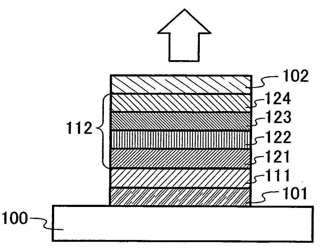
[0030]Embodiment Mode 1 will describe a light-emitting element having a structure in which reflection of light entering the light-emitting element from outside (external light) is suppressed.

[0031]FIG. 1 illustrates a light-emitting element in which a first electrode 101 formed over a substrate 100, a second electrode 102 opposite to the first electrode 101, a first layer 111 and a second layer 112. The first layer 111 and the second layer 112 are formed sequentially over the first electrode 101, and are between the first electrode 101 and the second electrode 102.

[0032]The substrate 100 is used as a support of the light-emitting element. For the substrate 100, glass, plastic, or the like can be used, for example. Any material other than these materials may be used as long as it functions as the support of the light-emitting element. In addition, the substrate 100 may include a structure of an interlayer insulating film or the like. If light is extracted to the outside through the s...

embodiment mode 2

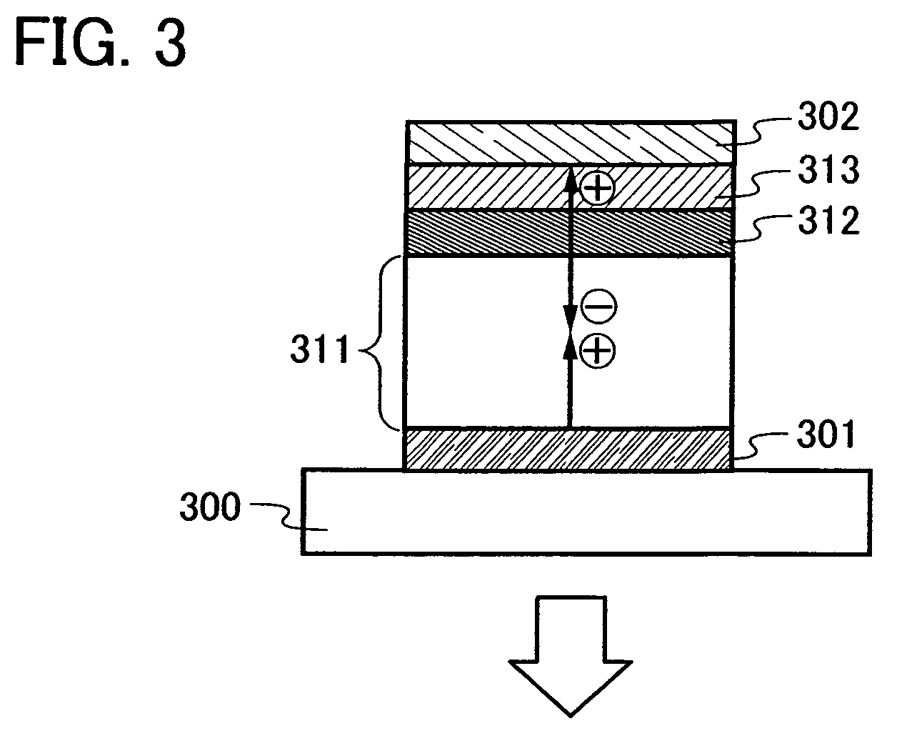
[0085]Embodiment Mode 2 will describe a light-emitting element with a structure different from the structure shown in Embodiment Mode 1. In this embodiment mode, a light-emitting element in which a light-absorbing layer is provided in contact with an electrode serving as a cathode is described with reference to FIG. 3.

[0086]FIG. 3 illustrates a light-emitting element in which a first electrode 301 formed over a substrate 300, a second electrode 302 opposite to the first electrode 301, and a first layer 311, a second layer 312 and a third layer 313 sequentially formed between the first electrode 301 and the second electrode 302 are provided.

[0087]In FIG. 3, the substrate 300 is used as a support of the light-emitting element. The substrate 300 can have a structure similar to the substrate 100 in Embodiment Mode 1.

[0088]In this embodiment mode, the light-emitting element includes the first electrode 301, the second electrode 302, and the first layer 311, the second layer 312 and the t...

embodiment mode 3

[0103]Embodiment Mode 4 will describe a light-emitting device including a light-emitting element of the present invention.

[0104]In this embodiment mode, a light-emitting device having the light-emitting element of the present invention in a pixel portion is described with reference to FIGS. 7A and 7B. It is to be noted that FIG. 7A is a top view showing the light-emitting device and FIG. 7B is a cross-sectional view taken along line A-A′ and B-B′ of FIG. 7A. This light-emitting device includes a driver circuit portion (source side driver circuit) 601, a pixel portion 602, and a driver circuit portion (gate side driver circuit) 603 in order to control the light emission of the light-emitting element. Also, a reference numeral 604 represents a sealing substrate, a reference numeral 605 represents a sealant, and the inside that is surrounded by the sealant 605 is a space 607.

[0105]A leading wiring 608 is a wiring for transmitting a signal to be inputted to the source driver circuit 601...


PUM


Abstract

The present invention provides a light-emitting element and a light-emitting device which have high contrast, and specifically, provides a light-emitting device whose contrast is enhanced, not by using a polarizing plate but using a conventional electrode material. Reflection of external light is suppressed by provision of a light-absorbing layer included between a non-light-transmitting electrode and a light-emitting layer. As the light-absorbing layer, a layer is used, which is obtained by adding a halogen atom into a layer including an organic compound and a metal oxide. Further, the light-absorbing layer is formed also over a region in which a thin film transistor for driving a light-emitting element is formed, a region in which a wiring is formed, and the like, and thus light is extracted from the side opposite to the region in which the TFT is formed, thereby reducing reflection of external light.

Description

BACKGROUND OF THE INVENTION[0001]1. Field of the Invention[0002]The present invention relates to a light-emitting element and a light-emitting device utilizing light emission such as electroluminescence, and a manufacturing method thereof. Further, the present invention relates to an electronic device having a light-emitting device.[0003]2. Description of the Related Art[0004]A display device including a light-emitting element (hereinafter, referred to as a light-emitting device) has advantages such as wide viewing angle, low power consumption, and high response speed as compared with a liquid crystal display device, and research and development thereof have been actively carried out.[0005]The light-emitting element has a light-emitting substance provided between a pair of electrodes, and light from the light-emitting substance is extracted depending on the light-transmitting property of the electrodes.[0006]For example, in a case where light is desired to be extracted in one direct...

Claims


Application Information

Patent Timeline
IPC IPC(8): H01L35/24H01L51/40
CPCH01L51/5284H01L51/5052H10K50/155H10K50/165H10K50/865H05B33/22H05B33/20H10K50/00
Inventor IBE, TAKAHIROIKEDA, HISAOKOEZUKA, JUNICHIKATO, KAORU
Owner SEMICON ENERGY LAB CO LTD
Why Eureka
Try Eureka