

Semiconductor device
a technology of semiconductor devices and transistors, applied in semiconductor devices, digital storage, instruments, etc., can solve the problems of difficult to adjust the current drive power ration ( ratio) of the driver transistor, and the general difficulty of changing the height of the finfet to the other in terms of process
- Summary
- Abstract
- Description
- Claims
- Application Information
AI Technical Summary
Problems solved by technology
Method used
Image

Examples
first embodiment
(1) First Embodiment
[0051](a) Configuration
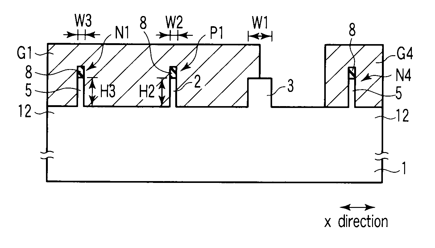
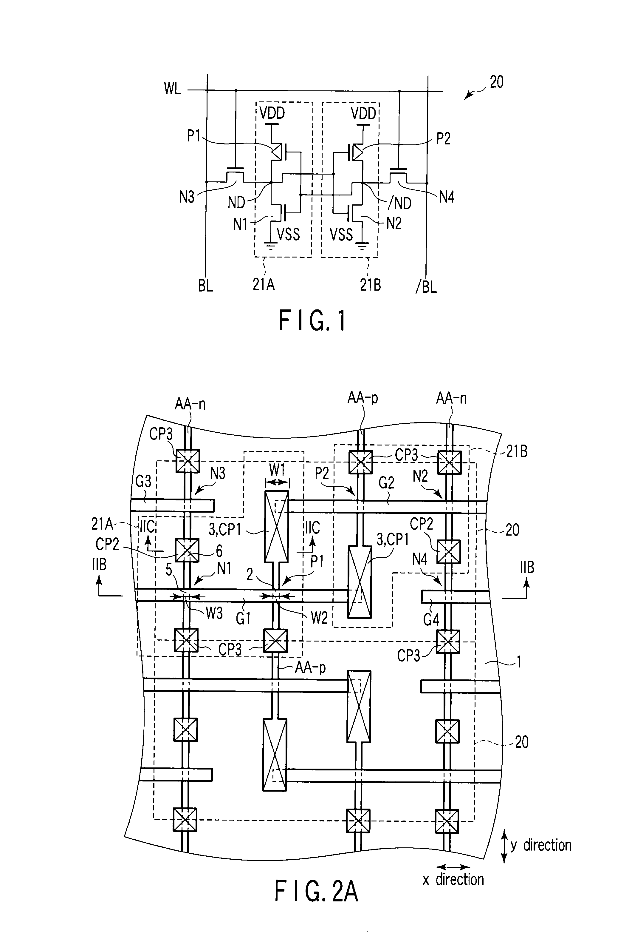
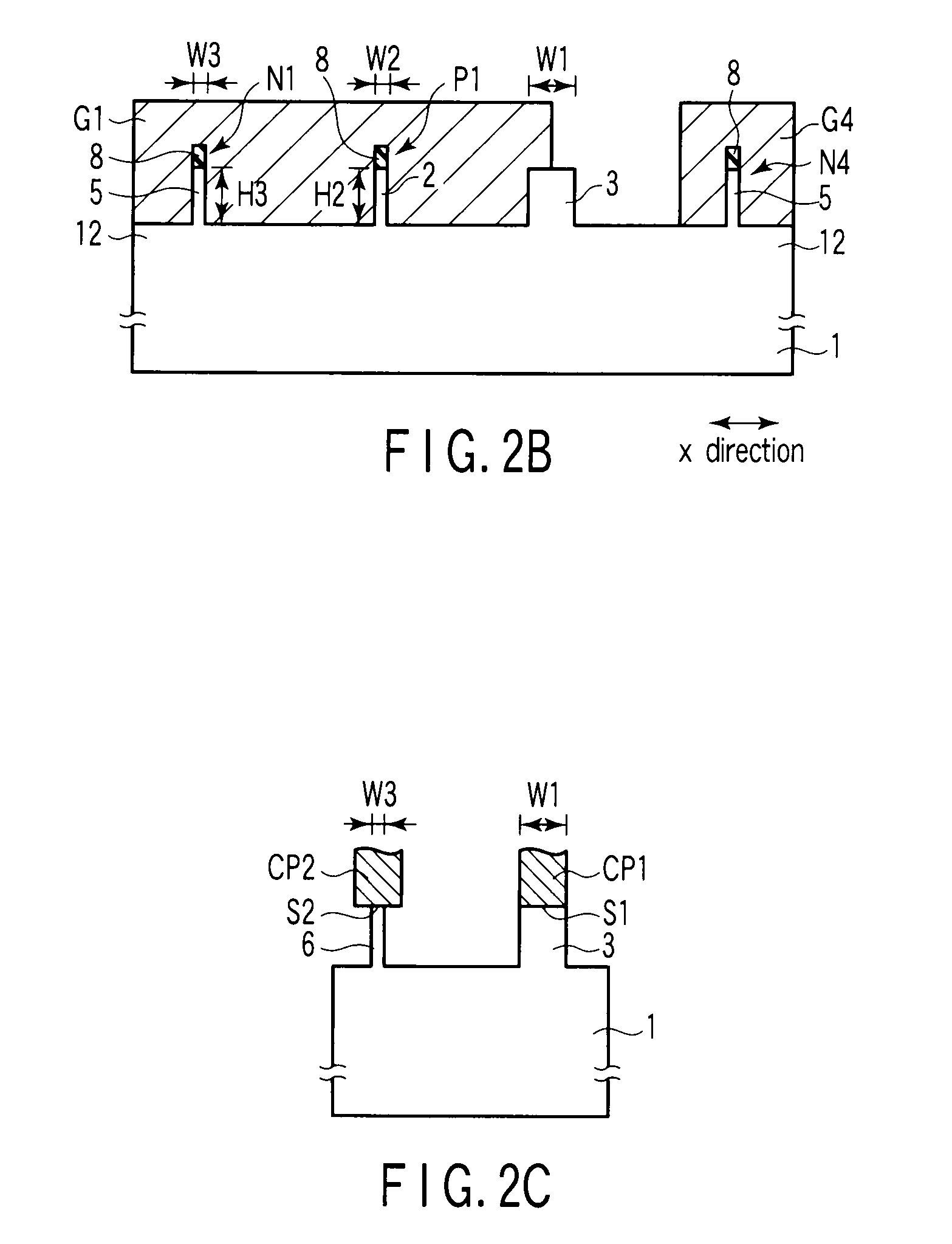
[0052]Using FIG. 1 to FIG. 2C, a first embodiment of the invention will be explained.
[0053]FIG. 1 is an equivalent circuit diagram of an SRAM cell 20. As shown in FIG. 1, the SRAM cell 20, which uses six MIS transistors as basic elements, is composed of two inverter circuits 21A, 21B connected so as to form a flip-flop to store data and transfer gate transistors for transferring data.
[0054]The inverter circuit 21A is composed of an n-type MIS transistor N1 and a p-type MIS transistor P1. In the SRAM cell 20, the n-type transistor N1 functions as a driver transistor and the p-type MIS transistor P1 functions as a load transistor. The drain of the n-type MIS transistor N1 is connected to the drain of the p-type MIS transistor P1. The connecting point between them is a node ND. Similarly, the inverter circuit 21B is also composed of an n-type MIS transistor N2 and a p-type MIS transistor P2. The n-type MIS transistor N2 functions as a driver t...
second embodiment
(2) Second Embodiment
[0096]Using FIGS. 5A and 5B, a second embodiment of the invention will be explained. In the second embodiment, the same parts as those in the first embodiment are indicated by the same reference numerals and a detailed explanation of them will be omitted.
[0097]In the inverter circuits 21A, 21B using the FinFETs of the first embodiment, the fin width W1 of the contact regions 3 of the p-type FinFETs P1 to P2 connected to the nodes ND, / ND is wider than each of the fin widths W2, W5 of the n- and p-type FinFETs N1 to N4, P1 to P2.
[0098]The second embodiment is characterized in that not only the width W1 of the contact region 3 of the p-type FinFET but also the width W2A of the channel region 2A of the fin acting as the active region of the p-type FinFET are wider than the width W3 of the channel region of the n-type FinFET.
[0099]In the examples of FIGS. 5A and 5B, the width W1 of the contact region 3 is the same as the width W2A of the channel region 2A and the wh...
third embodiment
(3) Third Embodiment
[0114]Using FIGS. 6A and 6B, a third embodiment of the invention will be explained. In the third embodiment, the same parts as those in the first and second embodiments are indicated by the same reference numerals and a detailed explanation of them will be omitted.
[0115]The third embodiment is characterized in that an n-well region N-well is further provided in the semiconductor substrate 1 in addition to the configuration of the second embodiment and that a p-type FinFET is arranged in the n-well region N-well.
[0116]The impurity concentration in the n-well region N-well is, for example, about 1017 / cm3 to 1018 / cm3. In this case, a p-well region P-well is provided in the semiconductor substrate 1 in a region where an n-type FinFET is arranged.
[0117]Since an ordinary FinFET is a fully depletion-mode MIS transistor, a change in the electric characteristics caused by a substrate bias is small.
[0118]However, in the p-type FinFETs P1, P2 of the third embodiment, the fi...
PUM
 Abstract
Description
Claims
Application Information