
Method of verifying semiconductor integrated circuit and design program

a technology of integrated circuit and design program, which is applied in the field of verification of semiconductor integrated circuits, can solve problems such as error detection, difficulty in performing lvs verification, and control cell failure to operate normally, and achieve the effects of preventing product deficiency caused by placement errors, reducing tat (turn around time), and improving production yield

Inactive Publication Date: 2008-12-18
RENESAS ELECTRONICS CORP
View PDF1 Cites 2 Cited by
  • Summary
  • Abstract
  • Description
  • Claims
  • Application Information

AI Technical Summary

Benefits of technology

[0016]As described above, it is possible according to the present invention to detect absence of the controlling cell required by the controlled cell, which can not be found by the conventional LVS verification. In other words, it is possible to check validity of the placement of the controlling cell and the controlled cell and to verify whether or not the controlled cell operates normally. As a result, product deficiency caused by a placement error can be prevented, which improves production yield.
[0018]According to the present invention, it is possible to verify validity of the placement of IO cells having a dependence relationship. Consequently, product deficiency caused by a placement error of the IO cells can be prevented, which improves production yield.

Problems solved by technology

Therefore, it has been difficult to perform the LVS verification in consideration of a power line and a ground line within the input-output buffer.
If the controlling cell is not placed in the region, the controlled cell can not operate normally.
Such a placement error should be detected during the layout design / verification stage.
However, the user netlist does not include information on the dependence relationship between the controlling cell and the controlled cell.
Therefore, it is not possible in the typical LVS verification to detect an error that the controlling cell required by the controlled cell does not exist.
If such a placement error is overlooked, a product does not operate normally.
In this case, a placement error of the IO cells can be detected prior to a power routing process and a cell placement / routing process.

Method used


Image

  • Method of verifying semiconductor integrated circuit and design program
  • Method of verifying semiconductor integrated circuit and design program
  • Method of verifying semiconductor integrated circuit and design program

Examples


first embodiment

1. First Embodiment

1-1. Design System and Operation

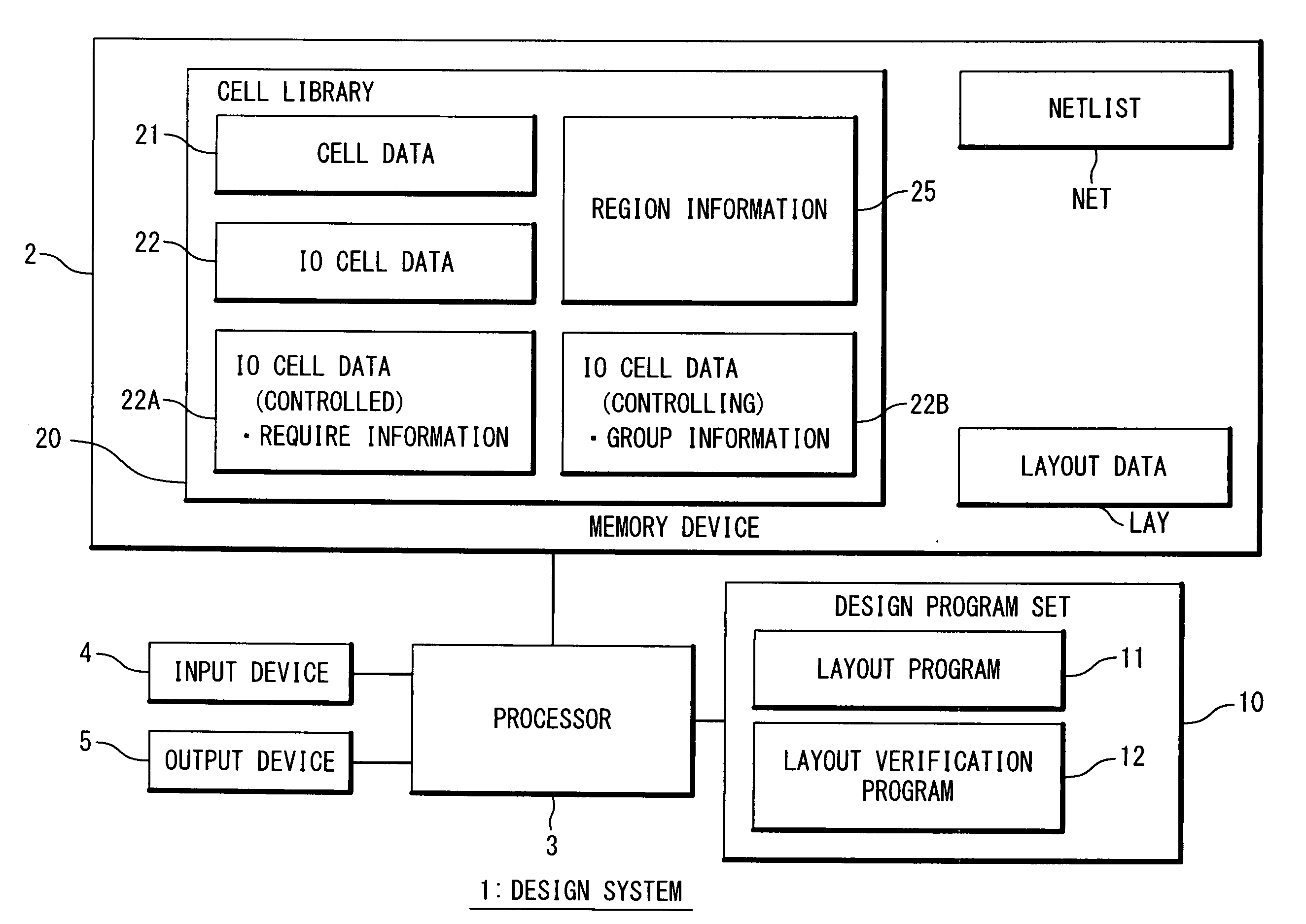
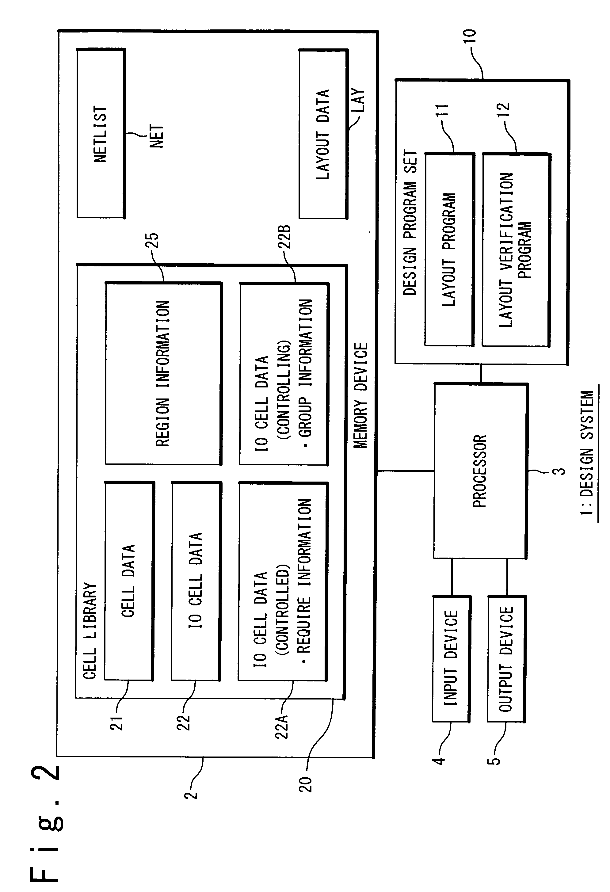
[0041]FIG. 2 is a block diagram showing a configuration example of a design system 1 according to a first embodiment of the present invention. The design system 1 is achieved by a computer system and includes a memory device 2, a processor 3, an input device 4, an output device 5 and a design program set 10. The memory device 2 includes a RAM and an HDD. The processor 3 controls operations of respective devices and executes data processing. The input device 4 includes a key board and a mouse. The output device 5 includes a display.

[0042]The design program set 10 is software executed by the processor 3 and includes a layout program11 and a layout verification program 12. These programs 11 and 12 may be recorded on a computer-readable recording medium and read out from the recording medium to the memory device 2. The designing of a semiconductor integrated circuit according to the present embodiment is achieved by cooperation of the p...

second embodiment

2. Second Embodiment

[0081]In a second embodiment of the present invention, a case of IOLH will be described as another example. The IOLH is a technique for achieving trimming of output impedance (driving capability) of an IO buffer.

2-1. IOLH

[0082]FIG. 12 is a circuit diagram for explaining the IOLH. A first IOLH buffer 51, a second IOLH buffer 52, a first IOLH controller 53, a second IOLH controller 54 and an IOLH enable cell 55 are the IO cells to be placed in the IO region.

[0083]The first IOLH buffer 51 is an IO buffer operating with 2.5 V. The second IOLH buffer 52 is an IO buffer operating with 3.3 V. The first IOLH controller 53 is a circuit for adjusting (trimming) the output impedance of the first IOLH buffer 51.

[0084]The second IOLH controller 54 is a circuit for adjusting the output impedance of the second IOLH buffer 52. The IOLH enable cell 55 is a circuit for activating the first IOLH controller 53 and the second IOLH controller 54.

[0085]The IO buffer (51, 52) includes a...

third embodiment

3. Third Embodiment

[0108]FIG. 18 is a block diagram showing a configuration example of a design system 1′ according to a third embodiment of the present invention. The description overlapping with the foregoing embodiments will be omitted as appropriate. In the present embodiment, the design program set 10 includes a layout program 11′ instead of the above-mentioned layout program 11. Also, a cell library 20′ instead of the above-mentioned cell library 20 is stored in the memory device 2. The cell library 20′ includes IO cell data 22′, 22A′ and 22B′ instead of the IO cell data 22, 22A and 22B.

[0109]As compared with the foregoing embodiments, “physical information” is further given to each of the IO cell data 22′, 22A′ and 22B′. The physical information indicates positions of terminals of interconnections included in the self-cell.

[0110]For example, FIG. 19 conceptually shows an IO cell related to the LVDS. The IO cell has an input terminal IN, an output terminal OUT, a power line VD...


PUM


Abstract

A method of verifying a semiconductor integrated circuit is provided. A controlling cell and a controlled cell controlled by a control signal output from the controlling cell are placed in an IO region of the semiconductor integrated circuit. The method includes: (A) providing a library that includes requirement information specifying the controlling cell required by the controlled cell; (B) obtaining a region information indicating a region within the IO region in which a signal interconnection through which the control signal is transmitted is provided; and (C) verifying whether or not the specified controlling cell is placed within the region, in a case where the controlled cell is placed within the region.

Description

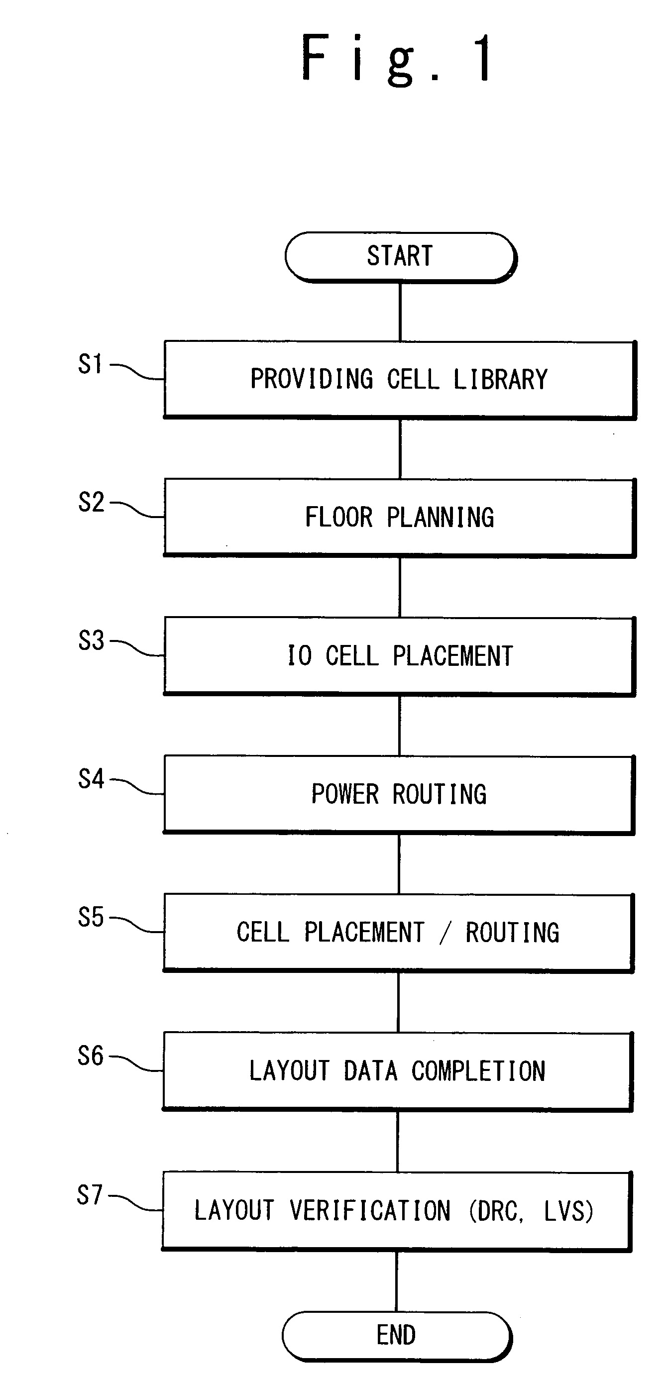
BACKGROUND OF THE INVENTION[0001]1. Field of the Invention[0002]The present invention relates to a technique of verifying a semiconductor integrated circuit. In particular, the present invention relates to a technique of verifying placement of IO cells in an IO region of a semiconductor integrated circuit.[0003]This application is based upon and claims the benefit of priority from Japanese patent application No. 2007-127577, filed on May 14, 2007, the disclosure of which is incorporated herein in its entirely by reference.[0004]2. Description of Related Art[0005]FIG. 1 is a flowchart showing a typical method of designing a semiconductor integrated circuit. First, a cell library is prepared (Step S1). The cell library consists of cell data of various kinds of cells. The various kinds of cells include a macro cell, a primitive cell, an IO cell and the like.[0006]Next, floor planning is performed based on a user netlist (Step S2). In the floor planning, locations of macro cells and pat...

Claims


Application Information

Patent Timeline
Patent Type & Authority Applications(United States)
IPC IPC(8): G06F17/50
CPCG06F17/5081H01L27/0203G06F30/398
Inventor OTSUKA, YASUO
Owner RENESAS ELECTRONICS CORP
Learn More