Method and apparatus for manufacturing electronic circuit board

a technology of electronic circuit board and manufacturing method, which is applied in the direction of manufacturing tools, instruments, conductive pattern formation, etc., can solve the problems of reducing the efficiency of manufacturing, and preventing the defect caused by erroneous application of laser beams

Inactive Publication Date: 2008-12-25
PANASONIC LIQUID CRYSTAL DISPLAY CO LTD +1
View PDF7 Cites 10 Cited by
  • Summary
  • Abstract
  • Description
  • Claims
  • Application Information

AI Technical Summary

Benefits of technology

[0012]According to the technology of the invention, defect is automatically corrected, and the effect of labor-saving is provided. Moreover, only defect which actually needs to be removed is corrected. As a result, the correction device is used with considerably higher efficiency, and defect caused by erroneous application of laser beam is prevented. Thus, reduction of manufacturing cost can be achieved.

Problems solved by technology

However, it is difficult to judge whether electric short-circuit has been actually caused or not through optical inspection.
In this case, there is a possibility that a foreign material only adhering to the TFT substrate on which the circuit is formed is erroneously judged as short-circuit defect, for example.
When laser beam is applied to the erroneously judged defect portion for removal of this portion based on erroneous judgment, defect is actually caused by cutting the normal circuit.
Furthermore, an electric inspection device only detects short-circuit and open-circuit between wirings and electrodes, and cannot specify the position (coordinates) of the defect causing short-circuit or open-circuit on the substrate.

Method used


Image

  • Method and apparatus for manufacturing electronic circuit board
  • Method and apparatus for manufacturing electronic circuit board
  • Method and apparatus for manufacturing electronic circuit board

Examples


first embodiment

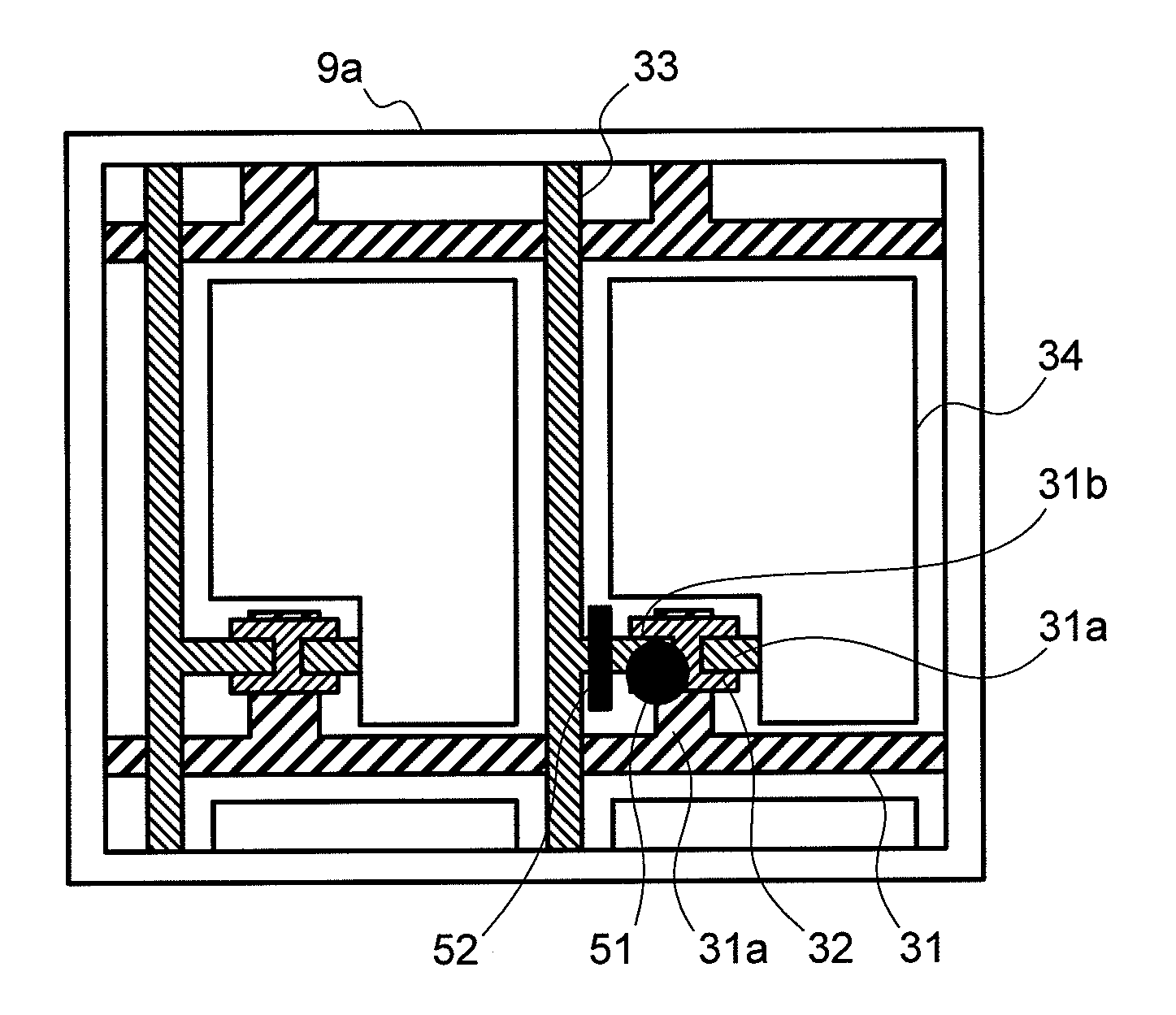
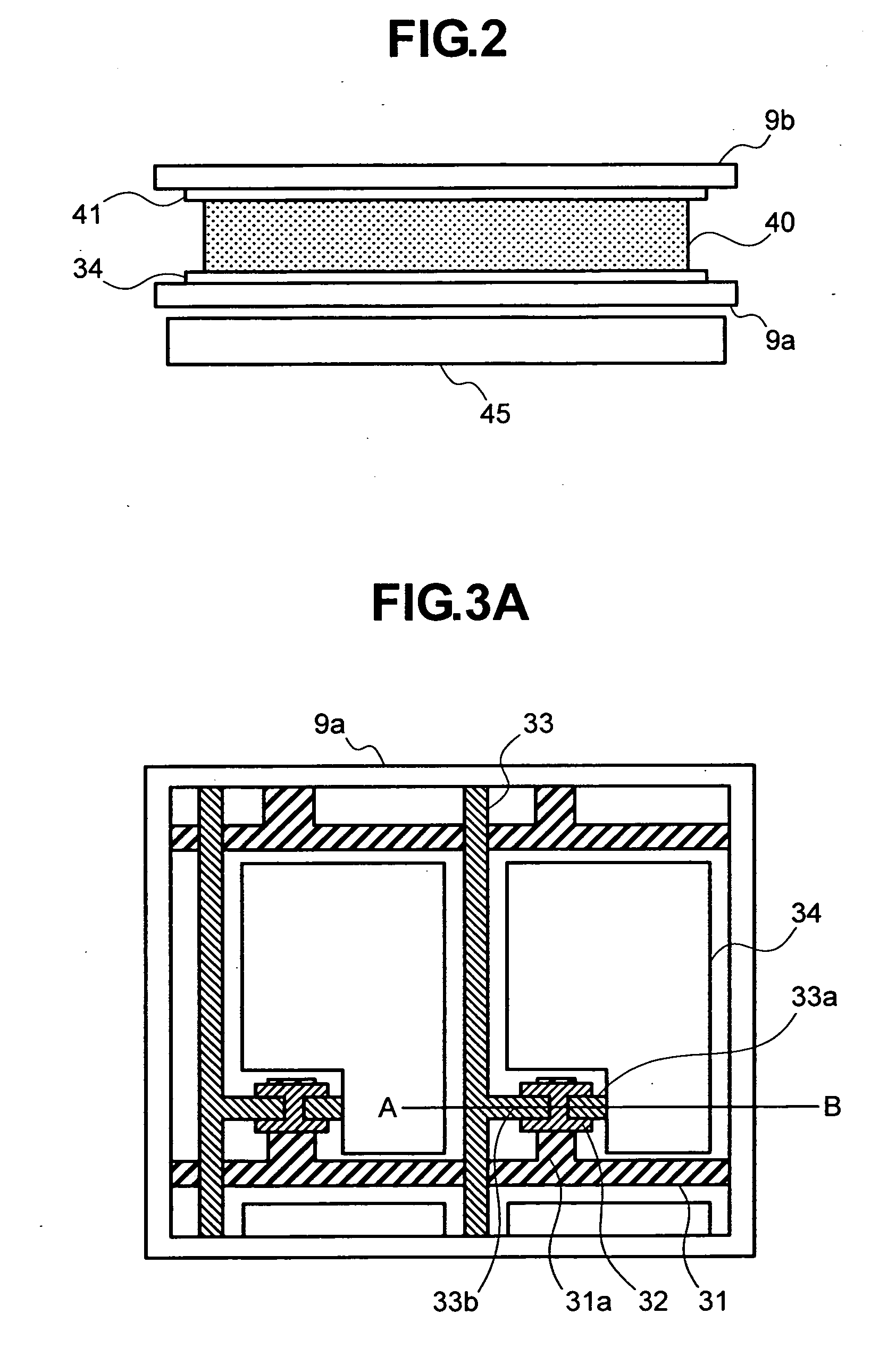
[0038]A first embodiment according to the invention is now described with reference to FIGS. 1 through 6B. FIG. 2 is a cross-sectional view of a typical liquid crystal display panel. This liquid crystal display panel has a liquid crystal 40 sandwiched between substrates 9a and 9b which are preferably formed by two sheets of glass. The liquid crystal display panel controls the direction (orientation) of liquid crystal molecules constituting the liquid crystal 40 by electric field generated by a pixel electrode 34 and an opposed electrode 41 within a capacitor to control light transmittance of a backlight 45. A circuit for controlling voltage applied to the pixel electrode 34 is provided on the substrate 9a, and a color filter is disposed on the substrate 9b so as to display a color image.

[0039]Since circuits constituted by thin film transistors such as pixel circuits and driving circuits are provided on the substrate 9a, the substrate 9a is called a thin film transistor substrate (TF...

second embodiment

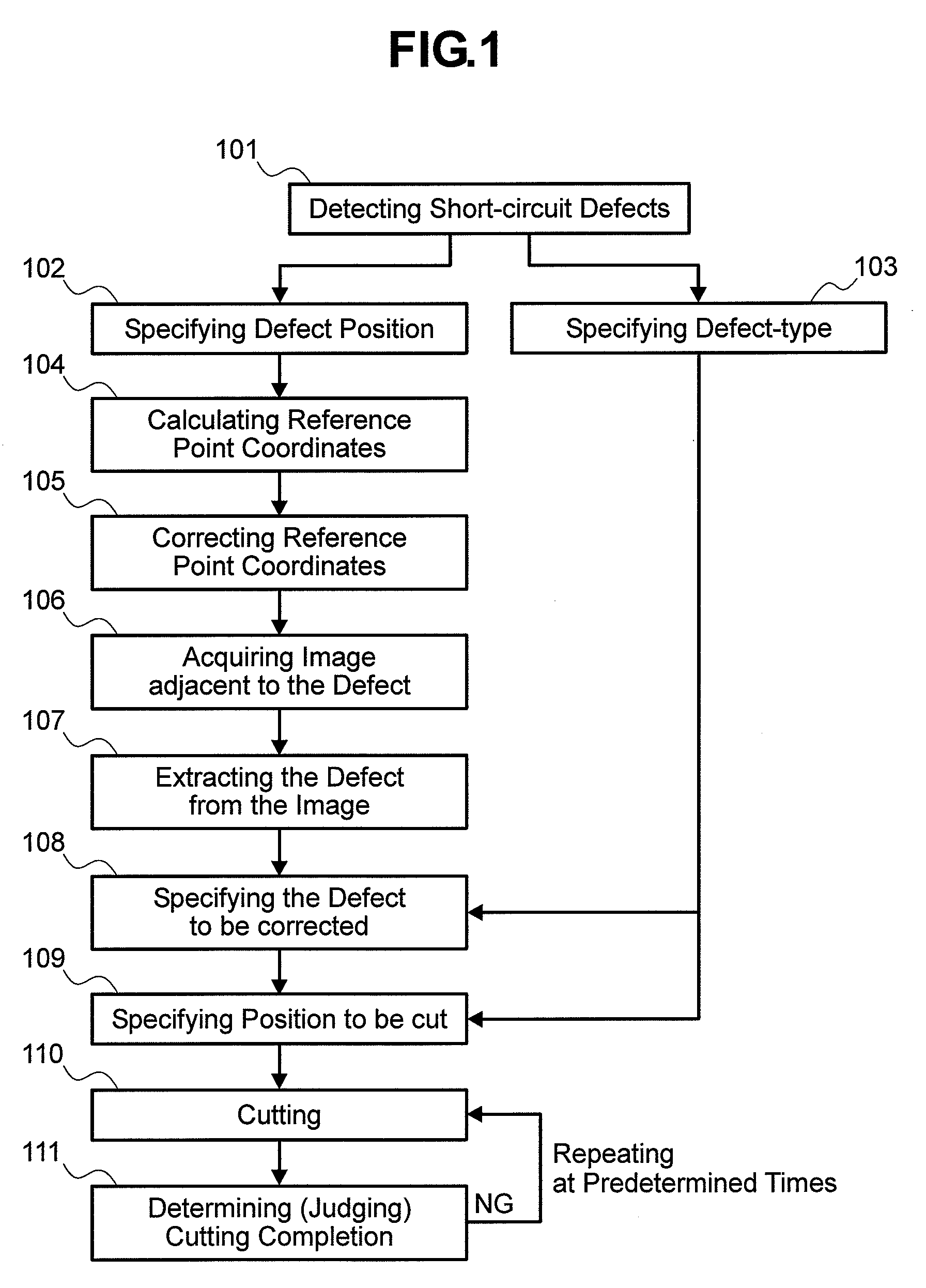
[0057]A second embodiment according to the invention is now described with reference to FIGS. 7 through 15. FIG. 7 illustrates a structure of a correction device included in a manufacturing apparatus for an electronic circuit board according to an example of the invention. This example is now discussed as the second embodiment of the invention. The correction device included in the manufacturing apparatus according to this embodiment has an inspection unit 200, a correction unit 230, and a memory unit 250. The inspection unit 200 is a unit for detecting short-circuit defect, and constituted by a short-circuit defect detecting part 201, a defect position specifying part 202, and a defect type specifying part 203.

[0058]The short-circuit defect inspection part 201 is a unit for attaching the probe 61 (61a and 61b in FIG. 4) to the pads of all the gate wirings 31 and data wirings 33, and measuring electric resistance between the gate wirings 31 and the data wirings 33, for example. The ...

third embodiment

[0073]A further embodiment of the invention is now described with reference to FIGS. 16 and 17. FIG. 16 illustrates a defect existing area according to a third embodiment of the invention. In this example, a plurality of defect existing areas 60a, 60b, 60c and 60d are defined. FIG. 17 shows a table for associating cutting positions with the defect existing areas. In FIG. 17, the table associates the cutting positions with defect types with one-to-one correspondence.

[0074]In case of the defect existing area 60 containing the plural defect existing parts as illustrated in FIG. 16, there is a possibility that a defect expands in the plural parts. In the condition where the cutting position 52 is stored in association with the defect existing area 60, the defect existing area 60a having the highest priority is selected by referring to the priorities given to the respective parts of the defect existing area 60. As a result, the cutting position 52a is determined. It is possible to define...


PUM

PropertyMeasurementUnit
defect typeaaaaaaaaaa
areaaaaaaaaaaa
defect imageaaaaaaaaaa

Abstract

A method for manufacturing an electronic circuit board which contains an electronic circuit on a main surface of a glass substrate according to the invention sequentially performs a step of electrically inspecting the main surface of the glass substrate on which the electronic circuit is formed, a step of specifying positions and defect types of defects on the main surface of the glass substrate, a step of calculating reference point coordinates on the main surface of the glass substrate and correcting the coordinates, a step of extracting respective defects from an image around the defects and specifying a defect to be corrected in the extracted defects by referring to a defect existing range registered in advance for each defect type, and a step of cutting the specified defect. By this method, a foreign material adhering to the glass substrate is not erroneously judged as short-circuit defect causing short-circuit on the electronic circuit, and only defect actually requiring correction can be removed.

Description

[0001]The present application claims priority from Japanese application JP2007-158314 filed on Jun. 15, 2007, the content of which is hereby incorporated by reference into this application.BACKGROUND OF THE INVENTION[0002]1. Field of the Invention[0003]The present invention relates to a method and an apparatus for manufacturing an electronic circuit board, and particularly to a technology for correcting short-circuit defect of an electronic circuit board on which repeated wirings and electrode patterns are formed.[0004]2. Description of the Related Art[0005]Currently, there is a heavy demand for cost reduction of a liquid crystal display panel with expansion of its market. On the other hand, the size of a glass substrate required for the manufacture of the liquid crystal display panel becomes larger and larger every year. In this situation, it is difficult to produce such a liquid crystal display panel causing no short-circuit defect only by process improvement, which is one of the ...

Claims


Application Information

Patent Timeline
Patent Type & Authority Applications(United States)
IPC IPC(8): H05K3/00H05K3/36
CPCG02F1/136259G02F2001/136254H01L27/12H05K3/225H01L27/124Y10T29/53004Y10T29/515Y10T29/49124Y10T29/49155Y10T29/49128Y10T29/49156Y10T29/49126G02F1/136254
Inventor NAKASU, NOBUAKI
Owner PANASONIC LIQUID CRYSTAL DISPLAY CO LTD
Why Eureka
Try Eureka