Method of manufacturing ZnO-based this film transistor

a thin film transistor and zno-based technology, applied in the direction of basic electric elements, electrical apparatus, semiconductor devices, etc., can solve the problems of reducing reliability, affecting the performance of a-si tfts, and affecting the efficiency of a-si tfts, so as to achieve the effect of preventing or reducing damage to channel layers

Active Publication Date: 2008-12-25
SAMSUNG ELECTRONICS CO LTD
View PDF4 Cites 94 Cited by
  • Summary
  • Abstract
  • Description
  • Claims
  • Application Information

AI Technical Summary

Benefits of technology

[0012]Example embodiments provide a method of manufacturing a ZnO-based thin film transistor (TFT) which may effectively prevent or reduce damage to a channel layer.

Problems solved by technology

However, because displays become larger and have higher image quality and thus driving and switching devices may also be required to have increased performance, existing a-Si TFTs having a low electron mobility of approximately 0.5 cm2 / Vs may suffer from limitations.
The a-Si TFTs have another problem in that as they may be operated for a long time, the performance of the a-Si TFTs may be degraded, thereby lowering reliability.
For this reason, the a-Si TFTs may be more difficult to be applied to organic light emitting diodes (OLEDs), which emit light using continuously applied current, than to liquid crystal displays (LCDs).
However, in order to manufacture poly-Si TFTs, more processes than those required to manufacture a-Si TFTs may be required and additional equipment may be required.
Accordingly, because poly-Si TFTs may be economically inferior to a-Si TFTs although the poly-Si TFTs may be suitable for higher quality displays or OLEDs, the poly-Si TFTs may suffer from limitations as well.
Because poly-Si TFTs have not been manufactured on a relatively large substrate exceeding 1 m because of technical problems, e.g., equipment needs or undesirable uniformity, the poly-Si TFTs may be difficult to be applied to TVs, thereby making it more difficult for high performance poly-Si TFTs to survive and prosper in the market.
However, any definite method of manufacturing a GIZO TFT has not been suggested and there may be several technical problems in manufacturing.
However, carrier concentration in a ZnO-based semiconductor film including the GIZO semiconductor film may be sensitive to a change in oxygen concentration, and the physical and electrical properties of the ZnO-based semiconductor film may be affected by thermal and chemical shock.
The semiconductor film may suffer a defect, e.g., an oxygen vacancy, due to the decomposition of ZnO, resulting in an increase in the carrier concentration.
If the channel layer under the source and drain electrodes is lost or the gate insulating layer outside the source and drain electrodes is over-etched and lost in the process of forming the source and drain electrodes, the bottom gate GIZO-based TFT may suffer undesirable performance and non-uniformity.
The increase in the electrical conductivity may make it difficult to control the threshold voltage of the bottom gate GIZO-based TFT and may decrease an on-off current ratio Ion / Ioff.
However, such attempts have failed to correct the problems.
Also, when a passivation layer, which may be a protective layer of the GIZO-based TFT, is deposited after the source and drain electrodes are formed, the surface of the channel layer may be damaged by plasma again.

Method used


Image

  • Method of manufacturing ZnO-based this film transistor
  • Method of manufacturing ZnO-based this film transistor
  • Method of manufacturing ZnO-based this film transistor

Examples


Embodiment Construction

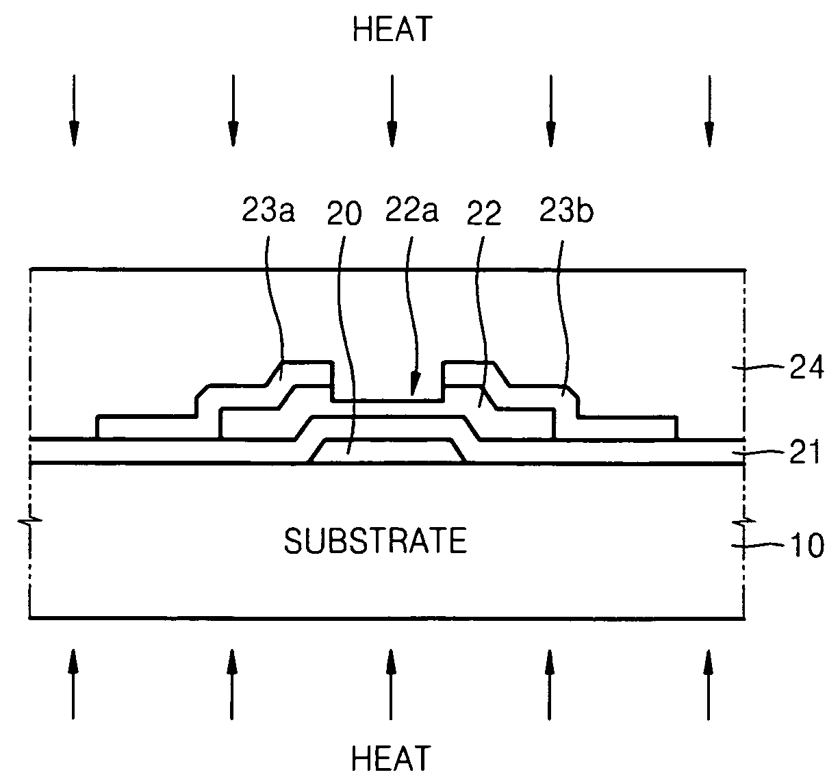
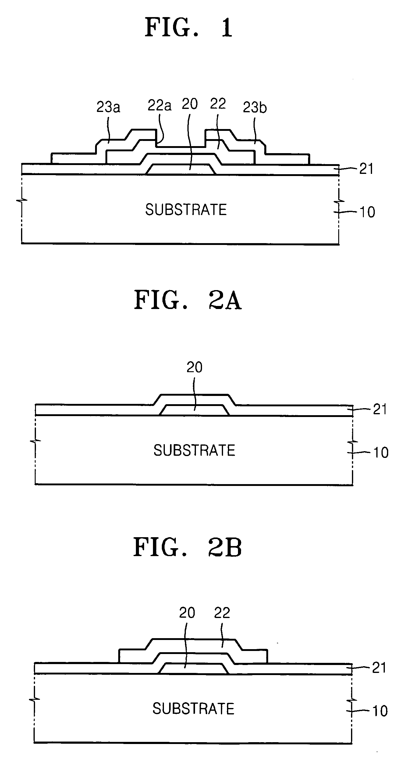
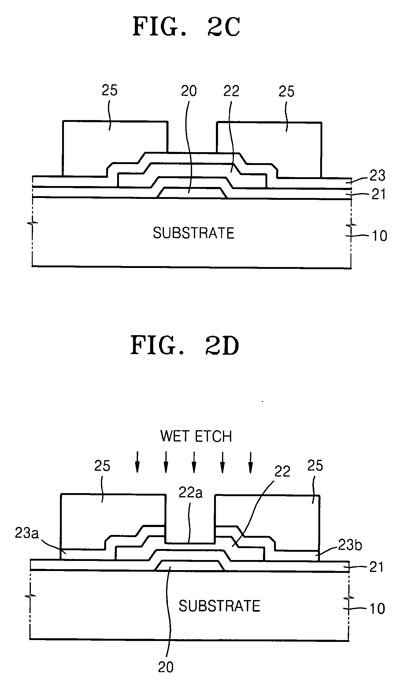
[0023]Example embodiments will now be described more fully with reference to the accompanying drawings, in which example embodiments are shown. In the drawings, the widths and thicknesses of layers or regions are exaggerated for clarity. Like reference numerals denote like elements in the drawings and repetitive description thereof will be omitted.

[0024]It will be understood that when an element is referred to as being “connected” or “coupled” to another element, it can be directly connected or coupled to the other element or intervening elements may be present. In contrast, when an element is referred to as being “directly connected” or “directly coupled” to another element, there are no intervening elements present. Like numbers indicate like elements throughout. As used herein the term “and / or” includes any and all combinations of one or more of the associated listed items.

[0025]It will be understood that, although the terms “first”, “second”, etc. may be used herein to describe ...


PUM


Abstract

Provided is a method of manufacturing a ZnO-based thin film transistor (TFT). The method may include forming source and drain electrodes using one or two wet etchings. A tin (Sn) oxide, a fluoride, or a chloride having relatively stable bonding energy against plasma may be included in a channel layer. Because the source and drain electrodes are formed by wet etching, damage to the channel layer and an oxygen vacancy may be prevented or reduced. Because the material having higher bonding energy is distributed in the channel layer, damage to the channel layer occurring when a passivation layer is formed may be prevented or reduced.

Description

PRIORITY STATEMENT[0001]This application claims priority under U.S.C. § 119 to Korean Patent Application No. 10-2007-0060685, filed on Jun. 20, 2007, and 10-2008-0019304, filed on Feb. 29, 2008, in the Korean Intellectual Property Office (KIPO), the entire contents of which are incorporated herein by reference.BACKGROUND[0002]1. Field[0003]Example embodiments relate to a method of manufacturing a ZnO-based thin film transistor (TFT), and more particularly, to a method of manufacturing a ZnO-based TFT which may effectively prevent or reduce damage to a channel layer.[0004]2. Description of the Related Art[0005]Televisions (TVs) may be the main applications of rapidly progressing flat panel displays. While liquid crystal displays (LCDs) are the most widely used displays for TVs, many attempts have been made to use organic light-emitting diodes (OLEDs) for TVs. The displays for TVs that have been developed are large screen, digital information display (DID), with relatively low cost, a...

Claims


Application Information

Patent Timeline
Patent Type & Authority Applications(United States)
IPC IPC(8): H01L21/00
CPCH01L29/7869
Inventor RYU, MYUNG-KWANLEE, SANG-YOONLEE, JE-HUNKIM, TAE-SANGKWON, JANG-YEONPARK, KYUNG-BAESON, KYUNG-SEOKJUNG, JI-SIM
Owner SAMSUNG ELECTRONICS CO LTD
Why Eureka
Try Eureka