Method of forming self-aligned gates and transistors

a technology of self-alignment and transistor, which is applied in the direction of semiconductor devices, basic electric elements, electrical equipment, etc., can solve the problems of inability to control variation, difficult control of the outline of the fin-typed gate structure in the lithography and etching process, and possible short circuit between the finfets

Inactive Publication Date: 2008-12-25
NAN YA TECH
View PDF0 Cites 23 Cited by
  • Summary
  • Abstract
  • Description
  • Claims
  • Application Information

AI Technical Summary

Problems solved by technology

For example, according to the conventional process of making the FinFET, the fin-typed gate structure is defined by a lithography and etching process, but the outline of the fin-typed gate structure is difficult to control in the lithography and etching process.
In addition, when the line width is smaller than 70 nm, the critical dimension variation cannot be controlled to be within a certain range, and a short circuit between the FinFETs may occur.

Method used


Image

  • Method of forming self-aligned gates and transistors
  • Method of forming self-aligned gates and transistors
  • Method of forming self-aligned gates and transistors

Examples


first embodiment

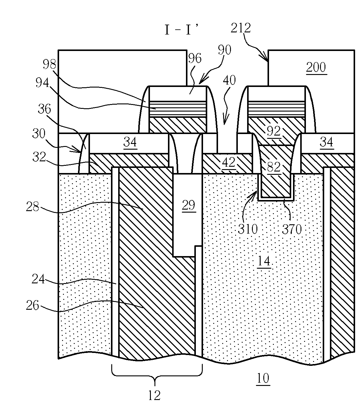
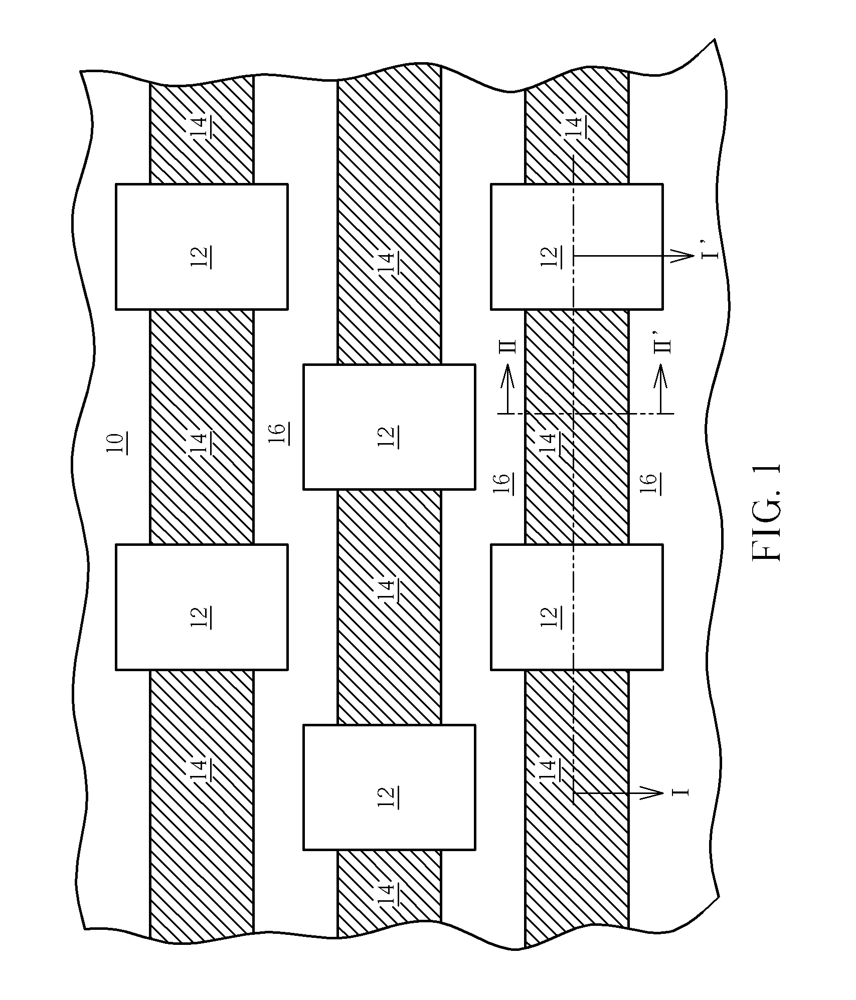
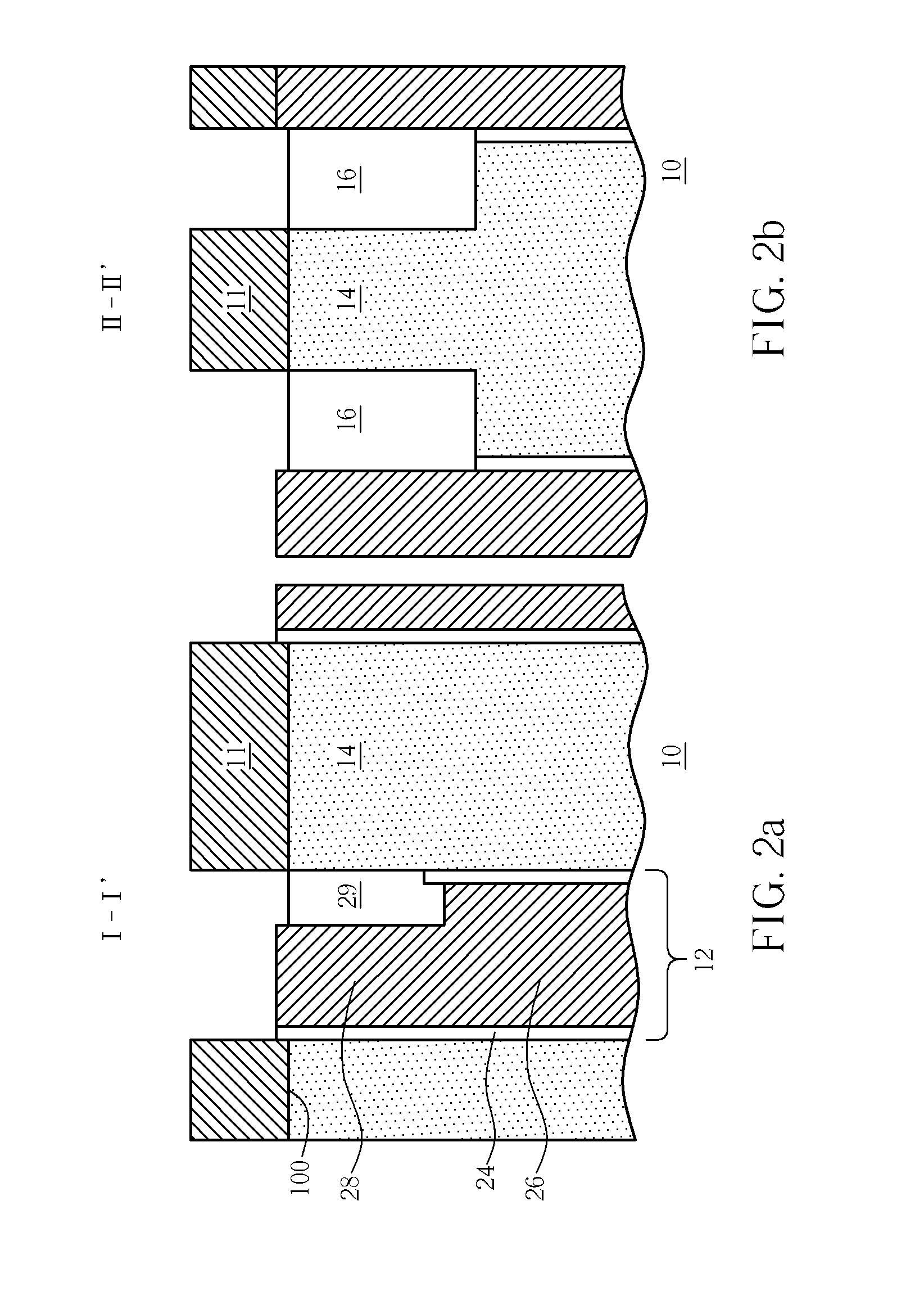
[0015]FIG. 1 to FIG. 14 depict a method for fabricating a FinFET according to the present invention. FIG. 1, FIG. 4, FIG. 7, FIG. 12 and FIG. 14 show a top view of a portion of a memory array. FIG. 2a, FIG. 2b, FIG. 3a, FIG. 3b, FIG. 5a, FIG. 5b, FIG. 6a, FIG. 6b, FIG. 8a, FIG. 8b, FIG. 9a, FIG. 9b, FIG. 10a, FIG. 10b, FIG. 11a, FIG. 11b and FIG. 13a, FIG. 13b depict a sectional view taken along the line I-I′ and II-II′ in FIG. 1. First, as shown in FIG. 1, FIG. 2a, and FIG. 2b, a substrate 10 covered by a pad nitride 11 comprises a plurality of deep trench capacitors 12. The pad nitride 11 is served as an etching hard mask in the deep trench capacitor 12 forming process. An active area 14 is defined between two adjacent deep trench capacitors 12 and a pair of paralleled shallow trench isolation (STI) regions 16. The STI region 16 electrically isolating the active area 14 is filled with silicon oxide.

[0016]The deep trench capacitor 12 comprises a sidewall capacitor dielectric layer ...

second embodiment

[0028]FIG. 15 to FIG. 24 depict a method for fabricating a recessed gate and a transistor by a self-aligned process according to the present invention. The same elements and regions are given the same numerical numbers for brevity. First, as shown in FIG. 15, FIG. 16a and FIG. 16b, a substrate 10 covered by a pad nitride 11 comprises a plurality of shallow isolation regions (STI) paralleled to each other and plurality of deep trench capacitors 12. The pad nitride 11 is served as an etching hard mask in the deep trench capacitor 12 forming process. An active area 14 is defined between two adjacent deep trench capacitors 12 and two shallow trench isolation regions 16. The STI region 16 electrically isolating the active area 14 is filled with silicon oxide.

[0029]The deep trench capacitor 12 comprises a sidewall capacitor dielectric layer 24 and a doped polysilicon layer 26, wherein the doped polysilicon layer 26 serves as a top electrode or an inner electrode. In order to simplify the ...


PUM


Abstract

Method for fabricating a self-aligned gate of a transistor including: forming a plurality of deep trench capacitors in a substrate, concurrently forming a surface strap and a contact pad on a surface of the substrate, wherein a spacing between the surface strap and the contact pad exposes a portion of an active area, filling the spacing with a dielectric layer, forming a photoresist pattern on the substrate, wherein the photoresist has an opening situated directly above the spacing between the surface strap and the contact pad, etching away the dielectric layer and a portion of a shallow trench isolation region through the opening thereby forming an upwardly protruding fin-typed channel structure, forming a gate dielectric layer on the upwardly protruding fin-typed channel structure, and forming a gate on the gate dielectric layer.

Description

BACKGROUND OF THE INVENTION[0001]1. Field of the Invention[0002]The present invention relates to a semiconductor manufacturing process, and more particularly to a method of forming self-aligned gates, fin-typed transistors or recessed gate transistors. The present invention can be applied to fabricate high-density trench capacitor DRAMs.[0003]2. Description of the Prior Art[0004]A DRAM (Dynamic random access semiconductor memory) comprises a memory cell array. The memory cells positioned in columns are connected by word lines and the memory cells positioned in rows are connected by bit lines. A DRAM can be operated by using word lines and bit lines to read and program memory cells.[0005]In general, memory cells comprise selection transistors and storage capacitors. The selection transistor is usually a planar FET comprising two diffusion regions separated by a channel, and a gate positioned above the channel. In addition, a word line is connected to one of the diffusion regions and ...

Claims


Application Information

Patent Timeline
Patent Type & Authority Applications(United States)
IPC IPC(8): H01L21/8242
CPCH01L27/0207H01L27/10876H01L27/10879H01L29/66787H01L29/7851H10B12/053H10B12/056
Inventor LEE, TZUNG-HANCHENG, CHIH-HAOLEE, PEI-TZUCHEN, TE-YINLEE, CHUNG-YUAN
Owner NAN YA TECH
Why Eureka
Try Eureka