Silicon wafer and method for producing same

a technology of silicon wafers and silicon wafers, which is applied in the direction of crystal growth process, after-treatment details, and protective fluids, etc., can solve the problems of difficult to ensure the desired resistivity, the inability to avoid the use of crystals with a small diameter, and the inability to achieve the enhancement of the productivity of high-frequency diodes, etc., to achieve the effect of reducing the generation of oxygen donors in the device-production heat treatment and high quality

Active Publication Date: 2009-01-01
SUMCO CORP
View PDF6 Cites 5 Cited by
  • Summary
  • Abstract
  • Description
  • Claims
  • Application Information

AI Technical Summary

Benefits of technology

[0038]As a result, the inventor found that doping of the silicon wafer with carbon was effective for the enhancement of the generation of oxygen precipitation induced defects, and was also effective for the depression of generation of oxygen donors, especially thermal donors.
[0063]By the use of the silicon wafer of the present invention, generation of oxygen donors during the device-production beat treatment is effectively reduced, and occurrence of the oxygen precipitation induced defects can be controlled at a desirable state. Therefore, the silicon wafer has sufficient mechanical strength, and the oxygen precipitation induced defects are prevented from causing slip dislocations. By the use of such a silicon wafer in the production of a high frequency diode, it is possible to use the oxygen precipitation induced defects as recombination centers in the high resistivity layer interposed between the P type region and the N type region of the high frequency diode. Since it is not necessary to perform a further treatment for forming the recombination center (recombination center constituted of Au or Pt, or electron beam irradiation defects or the like) for controlling lifetime, it is possible to reduce the number of steps in the production process of the high frequency diode. Since the above-described silicon wafer has a sufficient ability for gettering and the resistivity is not deviated from the preferable range by the device-production heat treatment, it is possible to shorten the treatment time and reduce the production cost. Therefore, the silicon wafer provided by the present invention is preferably applicable for manufacturing of a high frequency diode which is inexpensive, has high quality, has a high resistivity layer having sufficiently high resistivity, and generates few noise.

Problems solved by technology

However, where a high-frequency diode is produced using a silicon wafer made of the FZ crystal, it is impossible to avoid the use of a crystal having a small diameter since it is difficult to produce a crystal having a large diameter by the FZ method.
Therefore, using the FZ crystal, it is impossible to expect the enhancement of the productivity of the high-frequency diode.
On the other hand, where a high-frequency diode is produced using a silicon wafer made of a CZ crystal which may have a large diameter, there have been the following problems.
Therefore, it has been difficult to ensure a desired resistivity because of the fluctuation of resistivity before and after the heat treatment in the device production process.
However, in a substrate of P type crystal having high resistance, generation of oxygen donors during the device heat treatment process increase the resistivity.
In addition, if the generation of the oxygen donors is further increased, the oxygen donors override the P type impurities and generate an inversion from P type to N type resulting in a decrease of resistivity.
However, the use of silicon wafer made of the CZ crystal produced by the MCZ method and having low interstitial oxygen concentration includes problems such as an increase of production cost because of the application of the magnetic field and deterioration of mechanical strength of the silicon wafer after the device heat treatment because of the low interstitial oxygen concentration.
In addition, since the device heat treatment of the silicon wafer having low interstitial oxygen concentration generates only a low density of oxygen precipitation induced defects, sufficient gettering ability could not be achieved in some cases.
Therefore, the following problems cannot be avoided.
Firstly, in the techniques described in Patent References 1 to 3, since the residual interstitial oxygen concentration is extremely reduced by the generation of an excessive amount of oxygen precipitation induced defects, there is a problem that the silicon wafer has low mechanical strength.
The reduction of residual interstitial oxygen concentration of the silicon wafer may cause a deterioration of the mechanical strength of the silicon wafer.
However, this reduces the strength by acting as a source of slip dislocation and tends to generate wafer-warpage or the like under conditions of high heat and large dead weight stress (K. Sueoka et al., Jpn. J. Appl. Phys., 36(1997)7095: non-patent reference 2).
Therefore, there is a problem of the high production cost that accompanies the heat treatment.
Although the production cost may be depressed by the use of a general CZ crystal having a high interstitial oxygen concentration, high frequency diode as the final product is expensive.
Third, the techniques of Patent Reference 1 to 3 have problems of heavy metal contamination of the silicon wafer within the heat treatment furnace during the time of heat treatment.
Since the possibility of heavy metal contamination of the silicon wafer increases with increased heating time, there has been a high possibility of the silicon wafer suffering heavy metal contamination in the heat treatment furnace under the above-described heating condition with long duration.
Therefore, production of the high-frequency diode costed substantial labor and a high production cost.

Method used


Image

  • Silicon wafer and method for producing same
  • Silicon wafer and method for producing same
  • Silicon wafer and method for producing same

Examples


examples 1 through 4

[0101]A silicon single crystal having a crystal length of 1160 mm shown in FIG. 13 was grown by the CZ method and silicon wafers were sliced from the single crystal. From each of the Top, Middle, and Bottom portions of the crystal shown in FIG. 13, 50 mirror-polished wafers were obtained. The followings are the average values of resistivity, primary interstitial oxygen concentration, and carbon concentration of each portions: the Top portion had an resistivity of 980 Ωcm, primary interstitial oxygen concentration of 15.9×10¹⁷ atoms / cm3 (OLD ASTM), and carbon concentration of 4.8×10¹⁵ atoms / cm3; the Middle portion had a resistivity of 831 Ωcm, primary interstitial oxygen concentration of 14.6×10¹⁷ atoms / cm3 (OLD ASTM), and carbon concentration of 1.5×10¹⁶ atoms / cm3; and the Bottom portion had a resistivity of 599 Ωcm, primary interstitial oxygen concentration of 13.4×10¹⁷ atoms / cm3 (OLD ASTM) and carbon concentration of 5.9×10¹⁶ atoms / cm3.

[0102]Silicon wafers obtained from each porti...

example 5

[0104]A silicon single crystal having a resistivity of 1000 Ωcm, a primary interstitial oxygen concentration of 14.5×10¹⁷ atoms / cm3 (OLD ASTM) was grown by the CZ method. Silicon wafers sliced from the silicon single crystal were subjected to a beat treatment. Using a heat treatment furnace employing the lamp heating mechanism, beating temperature of the wafer was increased from 700° C. to 1000° C. with a heating rate of 5° C. / min. After the heat treatment, thermal stress of 4 MPa was applied to the wafers and occurrence of slip was examined in the same manner as in the above-described Examples 1 to 4. The results are shown in FIG. 9.

[0105]As shown in FIGS. 5 through 9, irrespective of the crystal portions of the silicon single crystal, wafers in Examples 2 through 4 heated with a heating rate of 1.0 to 2.0° C. / min showed fewer occurrences of slip compared with Example 5. Wafers in Example 3 heated with a heating rate of 1.5° C. / min showed fewer occurrences of slip compared with waf...

example 6

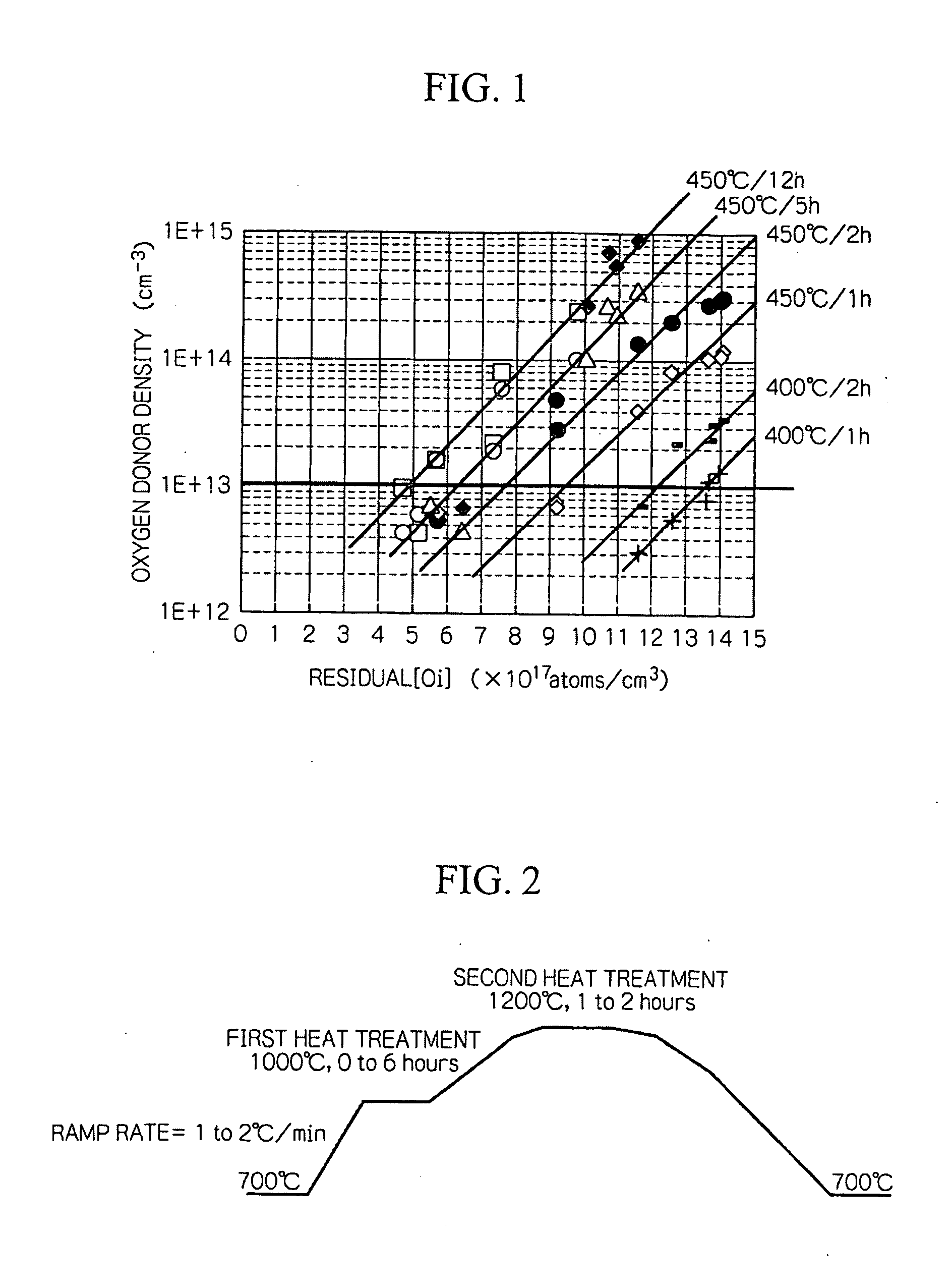
[0106]A silicon single crystal having a resistivity of 1000 Ωcm, primary interstitial oxygen concentration of 14.5×10¹⁷ atoms / cm3 (OLD ASTM), and a carbon concentration of 1.5×10¹⁶ atoms / cm3 was grown by the CZ method. Silicon wafers sliced from the silicon single crystal were subjected to a heat treatment. Using a heat treatment furnace employing the lamp heating mechanism, heating temperature of the wafer was increased from 700° C. to 1000° C. where the heating rate was selected from the various rates within the range of 1 to 2° C. / min and retained at 1000° C. for a duration selected from various durations in a range of 0 to 6 hours. After the heat treatment, relation between the heat treatment condition and residual interstitial oxygen concentration was examined. The results are shown in FIG. 10.

[0107]FIG. 10 is a graph showing the relation between a heating rate, a retention time at 1000° C., and a residual interstitial oxygen concentration (Res. [Oi]). As shown in FIG. 10, resi...


PUM

PropertyMeasurementUnit
resistivityaaaaaaaaaa
temperatureaaaaaaaaaa
resistivityaaaaaaaaaa

Abstract

A method for producing a silicon wafer that has a carbon concentration of 5×10¹⁵ to 5×10¹⁷ atoms / cm3, interstitial oxygen concentration of 6.5×10¹⁷ to 13.5×10¹⁷ atoms / cm3, and a resistivity of 100 Ωcm or more.

Description

[0001]This application is a divisional under 35 U.S.C. §§ 120 and 121 of U.S. patent application Ser. No. 11 / 699,894 filed Jan. 29, 2007 and titled SILICON WAFER AND METHOD FOR PRODUCING SAME, which is hereby incorporated by reference for all purposes.BACKGROUND OF THE INVENTION[0002]1. Field of the Invention[0003]The present invention relates to a high frequency diode, a silicon wafer that has high resistivity and preferably used in the high frequency diode, and a method for producing the silicon wafer. Priority is claimed on Japanese Patent Application No. No. 2006-022831 filed Jan. 31, 2006, the content of which is incorporated herein by reference.[0004]2. Description of Related Art[0005]Conventionally, PIN diodes, TRAPPATT diodes, and IMPATT diodes have been known as devices having a high resistivity layer (I layer: Intrinsic semiconductor layer) interposed between a PN junction, and are used as devices for high frequency switching. The high-resistivity layer is a drift region o...

Claims


Application Information

Patent Timeline
Patent Type & Authority Applications(United States)
IPC IPC(8): C30B33/02
CPCC30B15/00C30B33/02C30B29/06H01L21/20H01L21/22H01L21/324
Inventor KURITA, KAZUNARI
Owner SUMCO CORP
Why Eureka
Try Eureka