METHOD OF DOPING FIELD-EFFECT-TRANSISTORS (FETs) WITH REDUCED STRESS/STRAIN RELAXATION AND RESULTING FET DEVICES

a field-effect transistor and relaxation technology, applied in the fabrication and structure of metaloxidesemiconductor field-effect transistors (mosfet) devices, can solve the problems of short channel, current leakage, and large damage into the strained layers

Inactive Publication Date: 2009-01-01
GLOBALFOUNDRIES US INC
View PDF10 Cites 22 Cited by
  • Summary
  • Abstract
  • Description
  • Claims
  • Application Information

AI Technical Summary

Benefits of technology

[0012]These and other objects and features of the present invention are accomplished by performing halo / extension implantation into recessed silicon before forming the embedded strained region, thereby reducing the stress / strain relaxation in the embedded strained layers. The reduced relaxation is further accomplished by (in-situ) doping the source / drain region while, at the same time, forming the embedded strained layer by preferably separately epitaxially growing the layer. This provides for a higher activation of source / drain doping concentrations and reduces sheet resistance. An advantage of the present invention is that the fabrication process permits the use of adjusted dose / energy for the halo / extension dopants without changing the junction depth of the devices, herein CMOS devices.
is that the fabrication process permits the use of adjusted dose / energy for the halo / extension dopants without changing the junction depth of the devices, herein CMOS devices.

Problems solved by technology

With these miniature dimensions, however, performance problems of the devices result, such as short channel effects, punch through, and current leakage.
The implantation of all of these various dopants into the embedded strained layers (i.e.,—eSiGe and eSiC) generate a great amount of damage into the strained layers.
Damage relaxes the strained silicon (which is believed to be due to displacing the substitution strained dopants to the interstitial site which, in turn, reduces the strain / stress in the embedded strained eSiGe and eSiC layers in the source / drain regions and also further believed that strained silicon may experience relaxation via misfit / threading dislocation propagation).
This relaxation caused by implanted doping damage from the halo, extension and source / drain implantations into the embedded strained layers reduces the strain / stress in the embedded strained layers, which, in turn, reduces the strain / stress in the channel which, in turn, reduces the carrier mobility and degrades the device performance.
This creates a performance problem because the embedded strain layers in the source / drain region stress the channel and then create the respective strain / stress in the channel for carrier mobility.
However, the reduced source / drain stress causes reduction of channel stress and the reduced strain / stress in the channel, in turn, degrades the device performance because strain / stress in the channel is directly proportional to carrier mobility.

Method used


Image

  • METHOD OF DOPING FIELD-EFFECT-TRANSISTORS (FETs) WITH REDUCED STRESS/STRAIN RELAXATION AND RESULTING FET DEVICES
  • METHOD OF DOPING FIELD-EFFECT-TRANSISTORS (FETs) WITH REDUCED STRESS/STRAIN RELAXATION AND RESULTING FET DEVICES
  • METHOD OF DOPING FIELD-EFFECT-TRANSISTORS (FETs) WITH REDUCED STRESS/STRAIN RELAXATION AND RESULTING FET DEVICES

Examples


Embodiment Construction

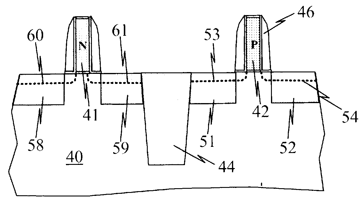
[0048]In accordance with the present invention, an improved fabrication process and semiconductor transistor device structure for FETs, such as pFETs (PMOS), nFETs (NMOS) and CMOS will be described. The process to be described enhances the transistor performance by reducing the stress / strain relaxation due to the damage accumulations from halo, extension, source / drain implantations into an embedded strained SiGe (eSiGe) for PMOS and an embedded strained SiC (eSiC) for NMOS layers or films in the source / drain region. Source and drain films or layers are made of an alloy of silicon and germanium and an alloy of silicon and carbon and, again in accordance with the present invention, by incorporating in-situ doping of boron or indium or the combination of both, during deposition, a higher active dopant concentration can be obtained than with implanted techniques, as well as reduced damage.

[0049]The eSiGe and eSiC alloys are epitaxially deposited on the layer of silicon. However, due to ...


PUM


Abstract

A method for fabricating a FET transistor for an integrated circuit by the steps of forming recesses in a substrate on both sides of a gate on the substrate, halo / extension ion implanting into the recesses, and filling the recesses with embedded strained layers comprising dopants for in-situ doping of the source and drain of the transistor. The stress / strain relaxation of the resulting transistor is reduced.

Description

FIELD OF THE INVENTION[0001]The present invention relates to the fabrication and structure of semiconductor devices and transistors and, more particularly, to the fabrication and structure of Metal-Oxide-Semiconductor Field-Effect-Transistors(MOSFET) devices, especially complementary FET or CMOS.BACKGROUND OF THE INVENTION[0002]The trend in semiconductor manufacture continues to be reducing the size of semiconductor devices while, at the same time, increasing their density on the chip. From a performance standpoint, the trend is to increase the speed of the devices and to reduce their power consumption. At the present time, the integrated circuit chips consist of billions of devices on each chip.[0003]To be able to reduce the size and density of the devices on the chip, the dimensions of the devices have to be made small. For example, the dimensions of the gate thickness and the source and drain of the FET now are in the micrometer and nanometer range. With these miniature dimension...

Claims


Application Information

Patent Timeline
Patent Type & Authority Applications(United States)
IPC IPC(8): H01L21/8238H01L29/778
CPCH01L21/823807H01L21/823814H01L29/7848H01L29/66636H01L21/823842
Inventor GAUTHIER, JR., ROBERT J.KRISHNASAMY, RAJENDRAN
Owner GLOBALFOUNDRIES US INC
Why Eureka
Try Eureka