Image sensor package utilizing a removable protection film and method of making the same

a protection film and image sensor technology, applied in the direction of photoelectric discharge tubes, instruments, radiation control devices, etc., can solve the problems of inability to meet the demand of producing smaller chips with high density elements on the chips, inability to manufacture packaging techniques, and inability to meet the demand of producing smaller chips with high density elements, etc., to achieve the effect of preventing particle contamination, promoting easiness and the highest yield, and no clean process

Inactive Publication Date: 2009-01-08
ADVANCED CHIP ENG TECH
View PDF1 Cites 35 Cited by
  • Summary
  • Abstract
  • Description
  • Claims
  • Application Information

AI Technical Summary

Benefits of technology

[0011]One advantage of the present invention is the removable protection film coated on the micro lens after the wafer fabs out and/or after the protection layer with water and oil repellency is coated.
[0012]Another advantage of the present invention is the removable protection film which can be temporarily struck on the micro lens area during the packaging and assembling process.
[0013]A still further advantage of the present invention is the removable protection film which can prevent any particle contamination on the micro lens area during the packag

Problems solved by technology

As semiconductor becomes more complicated, the traditional package technique, for example lead frame package, flex package, rigid package technique, can not meet the demand of producing smaller chip with high density elements on the chip.
Due to the conventional structure involved, this packaging technique may be expensive and difficult to manufacture.
Furthermore, because conventional package technologies have to divide a dice on a wafer into respective dies and then package the die respectively, therefore, these techniques are time consuming for manufacturing process.
Since the chip package technique is highly influenced by the development of integrated circuits, therefore, as the size of electronics has become demanding, so does the package technique.
Though the advantages of

Method used


Image

  • Image sensor package utilizing a removable protection film and method of making the same
  • Image sensor package utilizing a removable protection film and method of making the same
  • Image sensor package utilizing a removable protection film and method of making the same

Examples


Embodiment Construction

[0023]The invention will now be described in greater detail with preferred embodiments of the invention and drawings attached. However, it should be appreciated that the preferred embodiments of the invention are described only for illustrating but not for limiting the claims of the invention. Besides the preferred embodiments mentioned herein, the present invention can be practiced in a wide range of other embodiments besides those explicitly described, and the scope of the present invention is expressly not limited expect as specified in the accompanying claims.

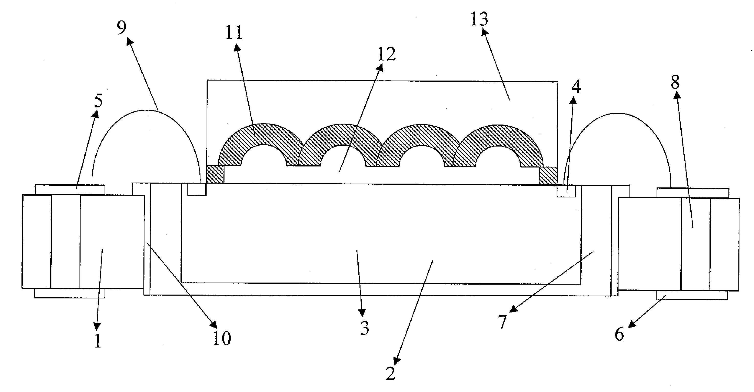
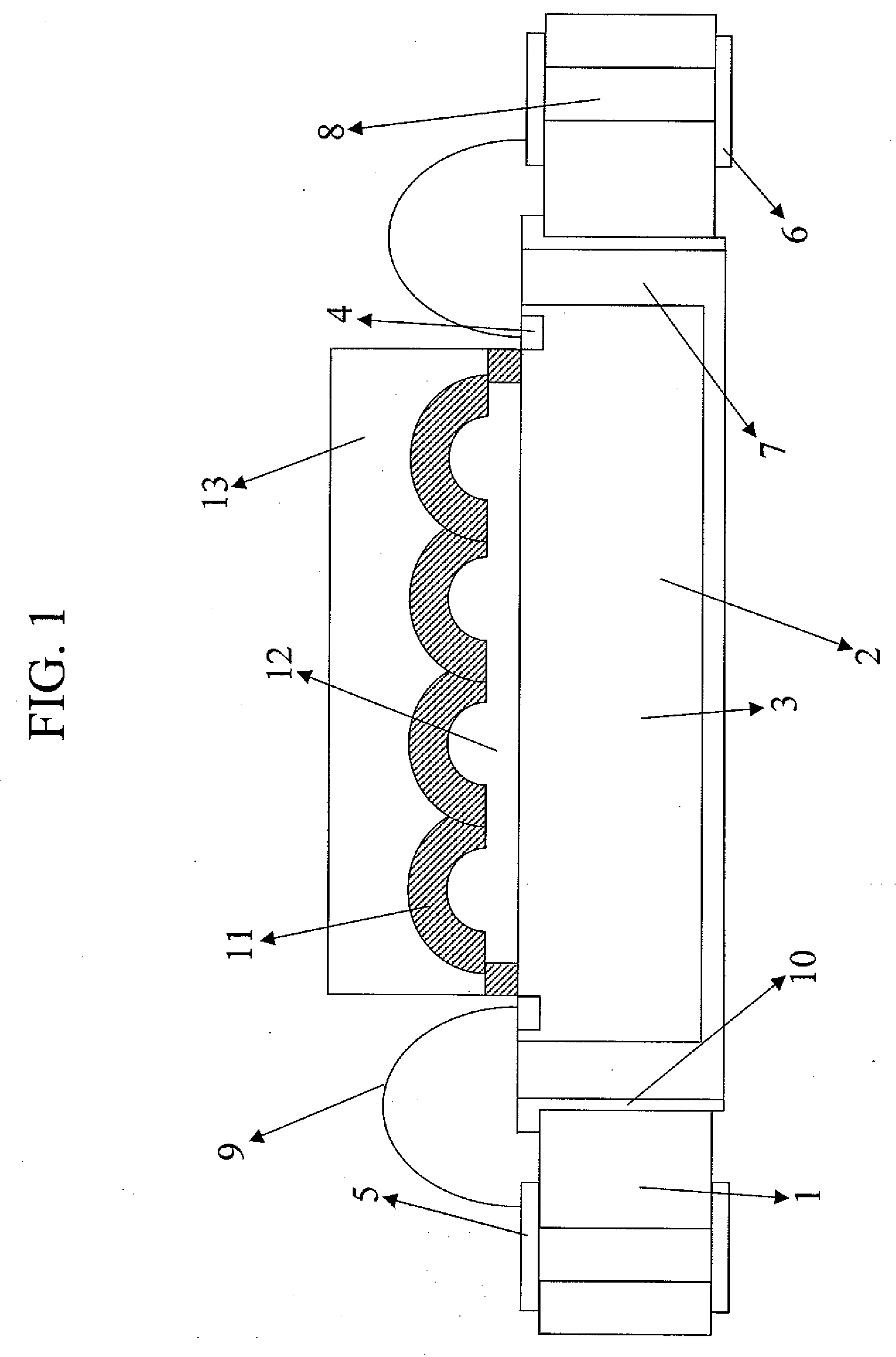
[0024]The present invention discloses a structure of an image sensor package utilizing a removable protection film. FIG. 1 illustrates a cross-sectional view of silicon wafer package of an image sensor in accordance with one embodiment of the present invention. As shown in FIG. 1, the structure of silicon wafer package includes a substrate 1 having a die receiving hole 2 formed therein to receive a die 3. The dimension of t...


PUM


Abstract

The present invention discloses a structure of image sensor package utilizing a removable protection film. The structure comprises a substrate with a die receiving cavity and inter-connecting through holes. Terminal pads are formed under the inter-connecting through holes and metal pads are formed on an upper surface of the substrate. A die is disposed within the die receiving cavity by an adhesion material. Bonding pads are formed on the upper edge of the die. Bonding wires are coupled to the metal pads and the bonding pads. A protection layer is formed on the micro lens area to protect the micro lens from particle contamination. A removable protection film is formed over the protection layer to protect the micro lens from water, oil, dust or temporary impact during the packaging and assembling process.

Description

FIELD OF THE INVENTION[0001]The present invention relates to a structure of an image sensor package, and more particularly, to a structure of an image sensor utilizing a removable protection film.BACKGROUND OF THE INVENTION[0002]In the field of semiconductor devices, the device density is increased and the device dimension is reduced continuously. The demand for the packaging or interconnecting techniques in such high density devices is also increased to fit the situation mentioned above. Conventionally, in the flip-chip attachment method, an array of solder bumps is formed on the surface of the die. The formation of the solder bumps may be carried out by using a solder composite material through a solder mask for producing a desired pattern of solder bumps. The function of chip package includes power distribution, signal distribution, heat dissipation, protection and support . . . and so on. As semiconductor becomes more complicated, the traditional package technique, for example l...

Claims


Application Information

Patent Timeline
IPC IPC(8): H01L31/0232H01L21/00
CPCH01L27/14618H01L27/14627H01L27/14687H01L2924/10253H01L2224/48091H01L2924/00014H01L2924/00H01L23/02H01L27/146
Inventor YANG, WEN-KUNCHANG, JUI-HSIENLEE, CHI-CHENYANG, WEN-PING
Owner ADVANCED CHIP ENG TECH
Why Eureka
Try Eureka