Electro-optical device and driving method for the same

a technology of optical devices and driving methods, applied in static indicating devices, non-linear optics, instruments, etc., can solve the problems of insufficient on-off action of tfts, inability to achieve high yield in such a situation, and difficulty in achieving grey tone display, etc., to reduce the photosensitivity of transistors and eliminate undesirable effects of incident ligh

Inactive Publication Date: 2009-01-08
SEMICON ENERGY LAB CO LTD
View PDF2 Cites 7 Cited by
  • Summary
  • Abstract
  • Description
  • Claims
  • Application Information

AI Technical Summary

Benefits of technology

[0016]In typical example, the present invention is applied to liquid crystal displays. Each pixel of the display is provided with a switching element of complimentary thin film field effect transistors which forcibly pull or push the level of the liquid crystal layer to a definite high or low voltage level rather than a floating state. Of course, the present invention can be practiced with a variety of other type transistors, other than thin film transistors, such as staggered types, coplanner types, inverted staggered types, inverted coplanner types. The channel regions of the transistors may b

Problems solved by technology

There are, however, undesirable cases in which the on-off action of the TFTs can not sufficiently carry out so that the output voltage of the TFT (i.e. the input to the pixel) reaches only short of a predetermined high voltage level (e.g. 5V), or the output voltage does not sufficiently fall to a predetermined low voltage (e.g. 0V).
In the case of the pane

Method used


Image

  • Electro-optical device and driving method for the same
  • Electro-optical device and driving method for the same
  • Electro-optical device and driving method for the same

Examples


first embodiment

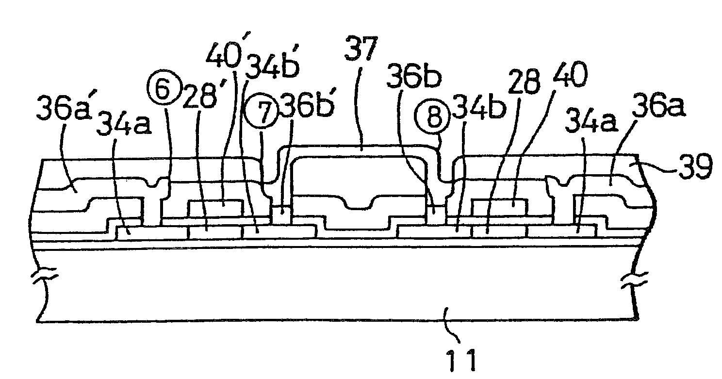
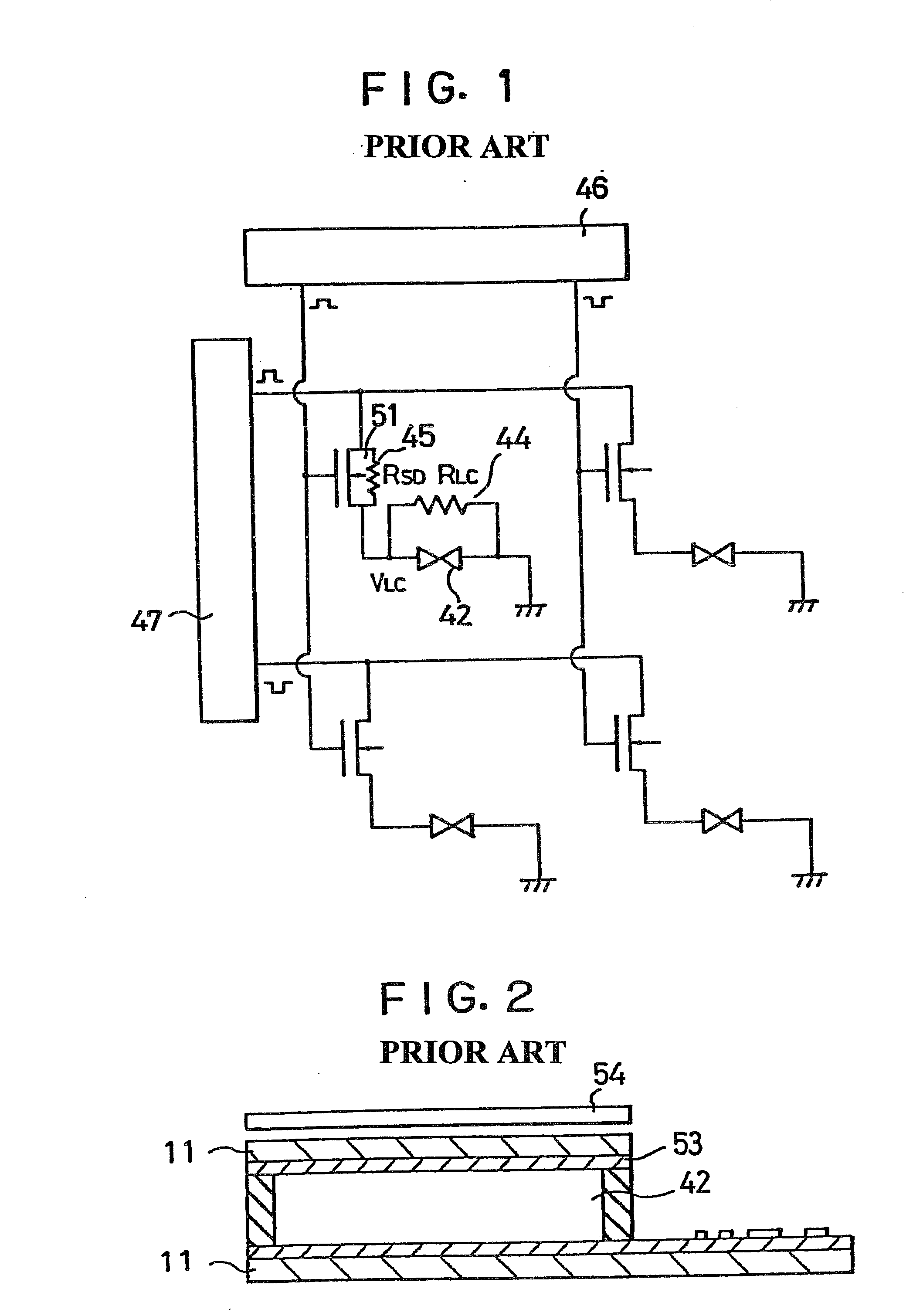
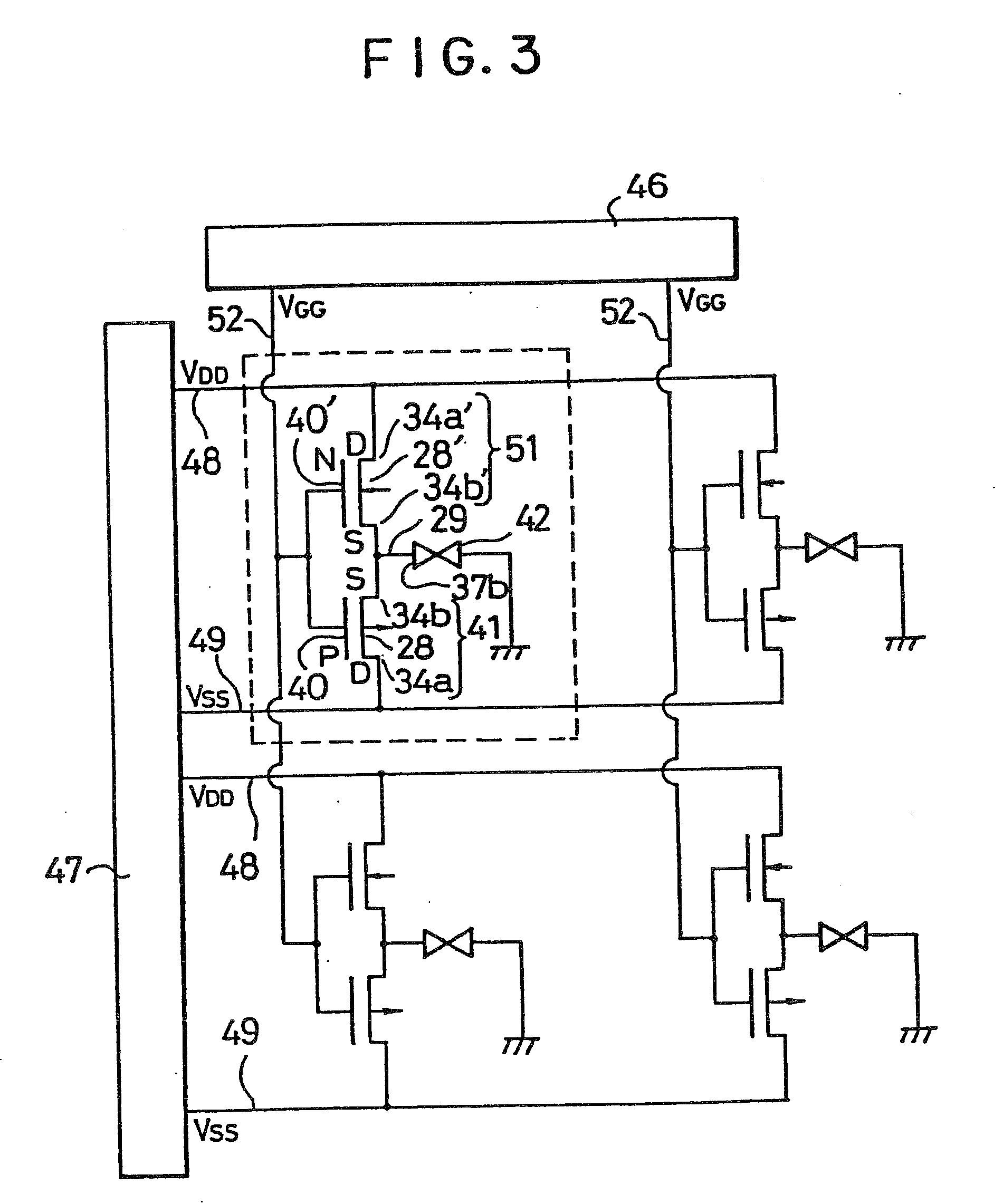
[0039]FIG. 3 is a diagram illustrating the equivalent circuit of a liquid crystal display in accordance with the present invention. The diagram shows only a 2×2 matrix for the sake of convenience in description whereas ordinary liquid crystal displays consist of more great numbers of pixels such as a 640×480 matrix, a 1260×960 matrix. The liquid crystal display includes a liquid crystal layer 42 disposed between a pair of glass substrates 11 and 11′ as shown in FIG. 2. The inner surface of the glass substrate 11′ is coated with an electrode 53. The inner surface of the other substrate 11 is provided with a plurality of conductive pads 37b each constituting one pixel of the display as seen from FIG. 4(A). Dashed line is enclosing one pixel in the figure. Each conductive pad 37b are formed on the substrate together with CMOS transistors consisting of an n-channel FET 51 and a p-channel FET 41 whose sources 34b′ and 34b are electrically connected with the corresponding pad 37b. The dra...

fourth embodiment

[0068]The representative example of the driving method in accordance with the present invention will be explained with reference to FIGS. 13 and 14. In FIG. 14, the 2×2 matrix of FIG. 11 is expanded to a 4×4 matrix. The configurations of them, however, are substantially identical except the number of pixels. FIG. 13 illustrates the control signals applied to the VD D lines, the VS S lines, the VG G lines and the back electrode. The VD D lines are called X1a, X2a, X3a and X4a from the first row to the forth row in the diagram whereas the Vss lines are called X1b, X2b, X3b and X4b in the same manner. The signals applied to the Vss lines are exactly the inversion of the signals to the VD D line and therefore the waveforms of the Vss lines are dispensed with in the illustration. The VG G lines are called Y1, Y2, Y3 and Y4 from the left column to the right column. In this driving method, the control signals applied to the VD D and Vss lines are addressing signals which scan from the firs...


PUM


Abstract

A grey tone display and a driving method are described. The display comprises a light influencing layer, an electrode pad located adjacent to the layer at one side of the layer in order to define a pixel in the layer, an n-channel field effect transistors connected to the electrode pad at its source terminal, a p-channel field effect transistors connected to the electrode pad at its source terminal, a first control line connected to the drain terminal of the n-channel field effect transistor, a second control line connected to the drain terminal of the p-channel field effect transistor, a third control line connected to the gate terminals of the n-channel field effect transistor and the p-channel field effect transistor, and a control circuit for supplying control signals to the first, second and third control lines. By this configuration, the voltage of the electrode pad can be arbitrarily controlled by adjusting the input level at the gate terminals.

Description

BACKGROUND OF THE INVENTION[0001]1. Field of the Invention[0002]The present invention relates to a grey tone display and a driving method for the same and, more particularly to a display driving system utilizing complimentary thin film gate insulated field effect transistors suitable for used in liquid crystal displays.[0003]2. Description of the Prior Art[0004]There have been well known in the art active liquid crystal displays which are driven by thin film transistors (TFTs). The displays of this type comprise visual panels and peripheral circuits for driving the panel. The peripheral circuit is formed by attaching a single crystalline chip containing integrated circuits on a glass substrate by tab-bonding or COG (chip on glass). The visual panel comprises a plurality of pixels each being provided with a driving TFT. The TFT is usually an N-channel FET formed within an amorphous or polycrystalline semiconductor film which is electrically coupled to a respective pixel.[0005]FIG. 1 ...

Claims


Application Information

Patent Timeline
IPC IPC(8): G09G3/36
CPCG02F1/13624G02F2001/134345G02F2001/136245G09G3/2011G09G2330/08G09G3/3648G09G2300/0426G09G2300/0809G09G2300/0823G09G3/3607G02F1/134345G02F1/136245
Inventor YAMAZAKI, SHUNPEIMASE, AKIRAHIROKI, MASAAKI
Owner SEMICON ENERGY LAB CO LTD
Why Eureka
Try Eureka