Substrate processing method, substrate processing system, and computer-readable storage medium

Active Publication Date: 2009-01-15
TOKYO ELECTRON LTD
View PDF3 Cites 19 Cited by
  • Summary
  • Abstract
  • Description
  • Claims
  • Application Information

AI Technical Summary

Benefits of technology

[0008]The present invention provides a substrate processing method in which damage of a low-k interlayer insulating film (a low-k film) after removal of a resist can be recovered sufficiently, and a substrate processing system for realizing the method, and a computer-readable storage medium storing a control program for executing the processing method.
[0009]As a result of several reviews for solving the problems, the present inventors have found that if a method of generating a hydrogen radicals from a hydrogen-containing gas by employing a catalyst and performing an ashing process on a resist film by using the hydrogen radicals is adopted, the degree of recovery from damage could be enhanced and damage at the time of an ashing process could be recovered sufficiently compared with the conventional plasma ashing employing an oxygen-containing gas when a recovery process employing a recovery gas such as a silylizing agent was subsequently performed on a low-k film.
[0016]In accordance with the present invention, a hydrogen radical is generated from a hydrogen-containing gas by employing a catalyst, an ashing process is performed on a resist film by using the hydrogen radical, and a recovery process employing a recovery gas such as a silylizing agent is performed on a low-k film. Accordingly, damage to the low-k film after removal of the resist can be recovered sufficiently.

Problems solved by technology

However, when ashing is performed by the plasma containing oxygen, there is a possibility that the low-k film may be damaged by oxygen radicals during the ashing process.
If such damage occurs, an etching shape is damaged and the k value also rises, so that the effects of the low-k film are deteriorated.
However, if ashing by using plasma of an oxygen-containing gas is performed for a long time, there is a problem in that the damage cannot be recovered sufficiently even though the silylation processing is performed.

Method used


Image

  • Substrate processing method, substrate processing system, and computer-readable storage medium
  • Substrate processing method, substrate processing system, and computer-readable storage medium
  • Substrate processing method, substrate processing system, and computer-readable storage medium

Examples


Embodiment Construction

[0025]Embodiments of the present invention will now be described with reference to FIGS. 1 to 7.

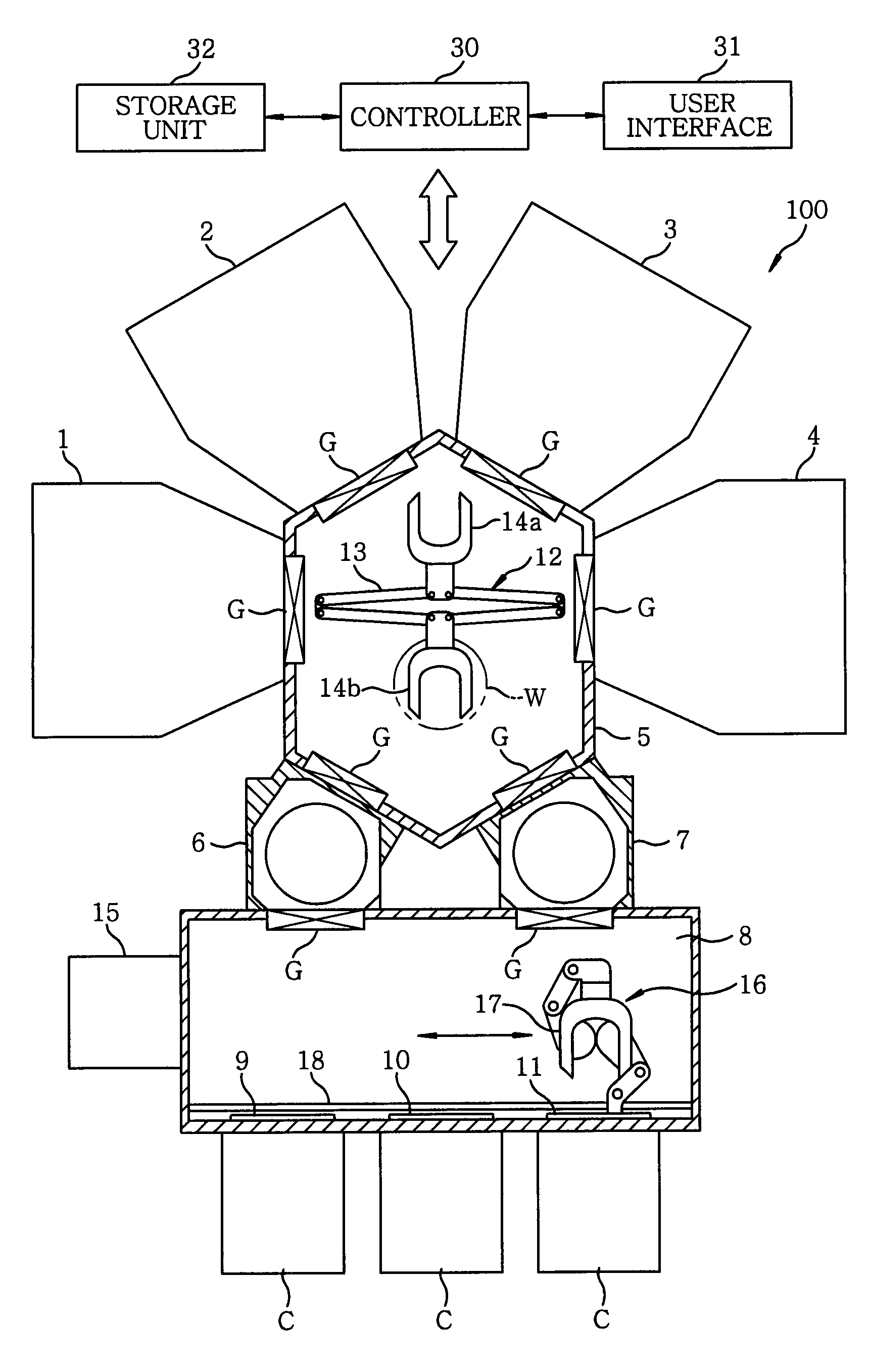
[0026]FIG. 1 is a schematic plan view illustrating a structure of a substrate processing system used to implement a substrate processing method in accordance with the present invention. The substrate processing system 100 is configured to process a semiconductor wafer W (a substrate) in which a photoresist film, as an etching mask having a predetermined circuit pattern, is formed on a low-k film (i.e., an etching target) by means of a photolithography process. The substrate processing system 100 includes etching units 1 and 2 for plasma etching, an ashing unit 3 for ashing, and a silylation processing unit 4. The units 1 to 4 are provided to correspond four sides of a wafer transfer chamber 5 having a hexagonal shape, respectively. Loadlock chambers 6 and 7 are provided on the remaining two sides of the wafer transfer chamber 5, respectively. A wafer loading / unloading chamber 8 is provide...


PUM

PropertyMeasurementUnit
Vacuumaaaaaaaaaa

Abstract

A substrate processing method includes preparing a substrate having a low-k interlayer dielectric film as a to-be-etched film and a photoresist film, formed on the low-k interlayer insulating film, serving as an etching mask with a predetermined circuit pattern; etching the low-k interlayer insulating film through the photoresist film to form grooves and / or holes in the low-k interlayer insulating film; ashing the photoresist film by using hydrogen radicals generated by bring a hydrogen-containing gas into contact with a catalyst of a high temperature; and recovering damage to the low-k interlayer insulating film due to the ashing by supplying a specific recovery gas. The method further includes recovering damage to the low-k interlayer insulating film due to the etching by supplying a specific recovery gas.

Description

FIELD OF THE INVENTION[0001]The present invention relates to a substrate processing method and a substrate processing system, in which etching is performed on a low-k interlayer dielectric film formed on a substrate by using a photoresist film having a predetermined circuit pattern as a mask, ashing is performed, and a recovery process using a recovery gas is performed.BACKGROUND OF THE INVENTION[0002]Recently, with an advancement of high speed, fine wiring pattern, and high density integration in semiconductor devices, there has been a request for decreasing a stray capacitance between wires and increasing a conductance of a wire to prohibit an increase of signal delay. A wire structure formed with a copper (Cu) wire having a low electrical resistance and an interlayer dielectric film of a low permittivity material, i.e., a low-k film has been widely used. In the era of a 45 nm half-pitch, a low-k film having a dielectric constant k of about 2.2 to 2.6 is required. Therefore, a por...

Claims


Application Information

Patent Timeline
IPC IPC(8): B44C1/22C23F1/08
CPCG03F7/427H01L21/31058H01L21/76831H01L21/76814H01L21/31138
Inventor TOMIOKA, KAZUHIROKOBAYASHI, NOBUYOSHISAKURAGI, ISAMUKUBOTA, KAZUHIRO
Owner TOKYO ELECTRON LTD
Why Eureka
Try Eureka