Electronics tester with a signal distribution board and a wafer chuck having different coefficients of thermal expansion

Active Publication Date: 2009-01-15
AEHR TEST SYST
View PDF9 Cites 30 Cited by
  • Summary
  • Abstract
  • Description
  • Claims
  • Application Information

AI Technical Summary

Benefits of technology

[0075]A pressure reduction passage may be formed through one of the components, the pressure reduction passage having an inlet opening at the pressure differential cavity and an outlet opening outside the pressure differential cavity, and a first valve in the component having the pressure reduction passage, further including opening of the first valve to allow air out of the pressure differential cavity, and closing the first valve, keeping air from entering the pressure differential cavity.
[0076]The first valve may be a check valve, a vacuum release passage being formed through the component having the check valve, the vacuum release passage having an inlet opening at the pressure differential cavity and an outlet opening outside the pressure differential cavity, and a second, vacuum release valve in the component having the vacuum release passage, further including: opening of the vacuum release valve to allow air into the pressure differential cavity, and closing of the valve, keeping air from escaping out of the pressure differential cavity.

Problems solved by technology

One challenge in full wafer testing is that there is a large amount of contacts on a wafer and that a large number of power, ground, and signal connections thus have to be made.
Another challenge is that burn-in testing requires a thermal management system that can maintain the wafer stable at a relatively high temperature, while providing a system that is simple to operate and relatively inexpensive.

Method used


Image

  • Electronics tester with a signal distribution board and a wafer chuck having different coefficients of thermal expansion
  • Electronics tester with a signal distribution board and a wafer chuck having different coefficients of thermal expansion
  • Electronics tester with a signal distribution board and a wafer chuck having different coefficients of thermal expansion

Examples


Embodiment Construction

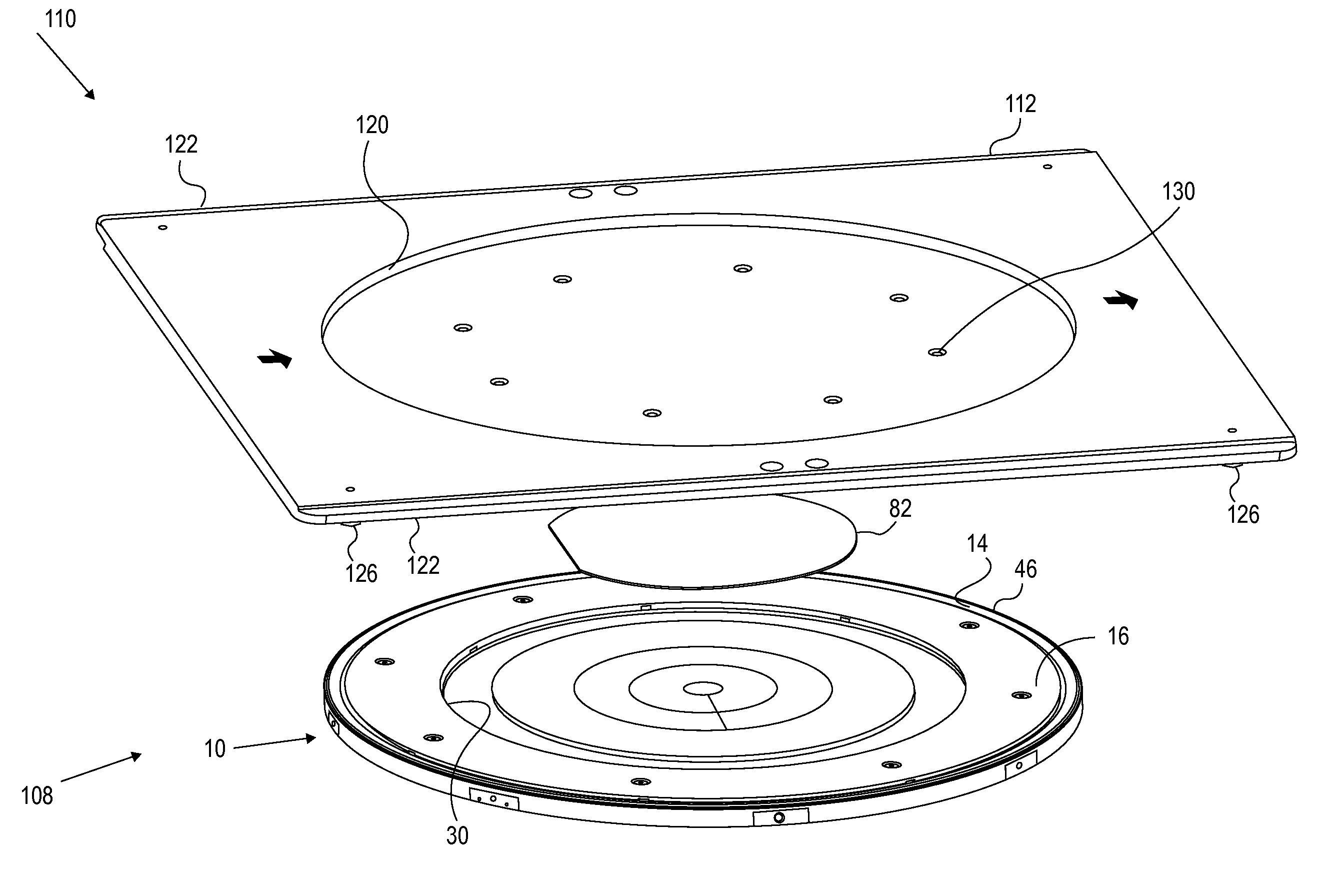
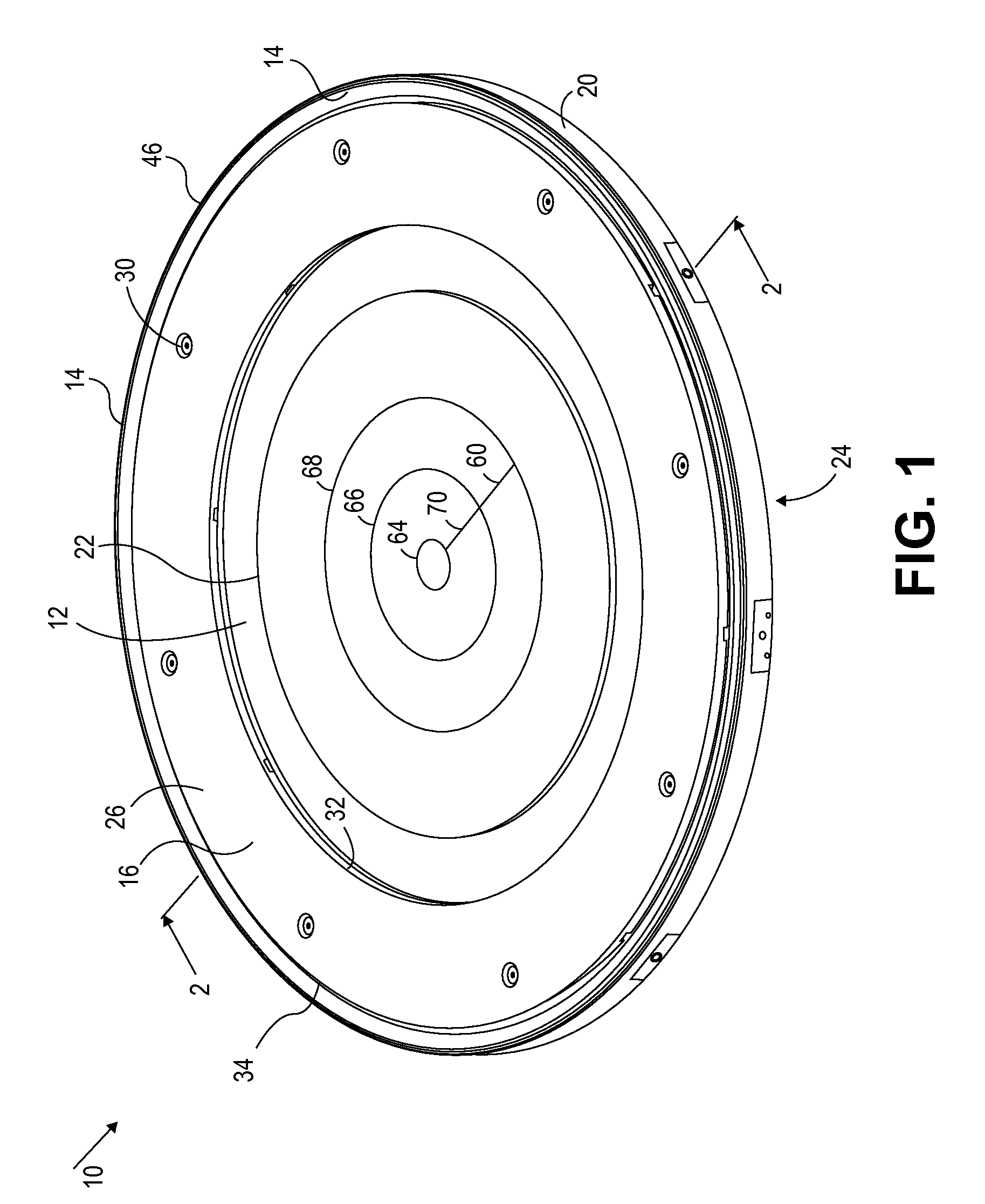
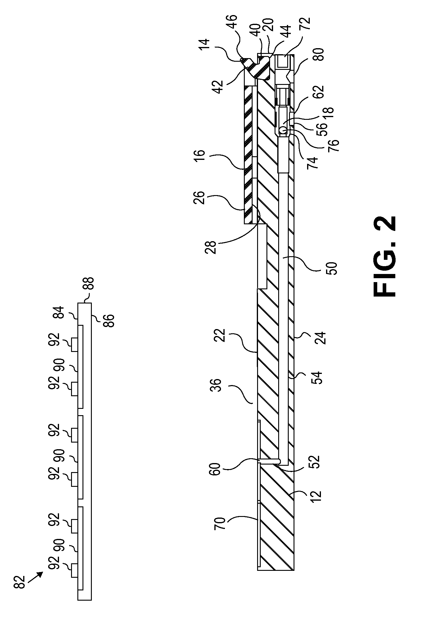
[0146]FIG. 1 of the accompanying drawings illustrates a wafer chuck assembly 10 in perspective view, and FIG. 2 illustrates a portion of the wafer chuck assembly 10 in cross-sectional side view. The wafer chuck assembly 10 includes a wafer chuck component 12, a pressure differential substrate cavity seal 14, an offset ring 16, and a substrate suction passage valve 18.

[0147]The wafer chuck component 12 is made of aluminum or another metal having relatively high thermal conductivity and has a predetermined, relatively low coefficient of thermal expansion. The wafer chuck component 12 has a circular outer surface 20 and upper and lower surfaces 22 and 24. The diameter of the outer surface 20 is typically between 350 and 450 mm, more typically approximately 400 mm. The upper surface 22 has a number of grooves formed therein and extends up to the outer surface 20. The lower surface 24 is also formed in a single plane that extends up to the outer surface 20. The planes of the upper and lo...


PUM


Abstract

The invention relates to a tester apparatus of the kind including a portable supporting structure for removably holding and testing a substrate carrying a microelectronic circuit. An interface on the stationary structure is connected to the first interface when the portable structure is held by the stationary structure and is disconnected from the first interface when the portable supporting structure is removed from the stationary structure. An electrical tester is connected through the interfaces so that signals may be transmitted between the electrical tester and the microelectronic circuit to test the microelectronic circuit.

Description

CROSS-REFERENCE TO RELATED APPLICATIONS[0001]This application claims priority from U.S. Provisional Patent Application No. 60 / 910,433, filed on Apr. 5, 2007, which is incorporated herein by reference in its entirety.BACKGROUND OF THE INVENTION[0002]1). Field of the Invention[0003]This invention relates to an apparatus that is used for full-wafer testing and / or burn-in testing and / or built-in self-testing.[0004]2). Discussion of Related Art[0005]Microelectronic circuits are usually fabricated in and on semiconductor wafers. Such a wafer is subsequently “singulated” or “diced” into individual dies. Such a die is typically mounted to a supporting substrate for purposes of providing rigidity thereto and electronic communication with an integrated or microelectronic circuit of the die. Final packaging may include encapsulation of the die and the resulting package can then be shipped to a customer.[0006]It is required that the die or the package be tested before being shipped to a custome...

Claims


Application Information

Patent Timeline
Patent Type & Authority Applications(United States)
IPC IPC(8): G01R31/3181
CPCG01R1/0491G01R31/2863G01R31/2879G01R31/2875G01R31/2865G01R31/2889G01R31/2856
Inventor STEPS, STEVEN C.LINDSEY, SCOTT E.DEBOE, KENNETH W.RICHMOND, II, DONALD P.CALDERON, ALBERTO
Owner AEHR TEST SYST
Why Eureka
Try Eureka