Structure of high power edge emission laser diode

a laser diode and high-power technology, applied in the direction of laser details, semiconductor lasers, electrical apparatus, etc., can solve the problems of low confinement factor, multi-mode oscillation, kink phenomenon, etc., and achieve good confinement factor, prolong life, and reduce vertical divergence angle

Inactive Publication Date: 2009-01-15
NAT CHIAO TUNG UNIV
View PDF2 Cites 2 Cited by
  • Summary
  • Abstract
  • Description
  • Claims
  • Application Information

AI Technical Summary

Benefits of technology

[0009]To solve the aforementioned problems, one object of the present invention is to provide a structure of a high power edge emission laser diode that has plural mode extension sublayers with a chirp periodic distribution, and which Near Field Pattern (NFP) is an L shape and which high intensity portion is nicely overlapped with the multi quantum wells to obtain a good confinement factor. Furthermore, the low intensity portion will extend to the n-type cladding layer as it can as possible. Accordingly, the optical power density on the mirror surface of the high power edge emission laser diode is lowered down and the vertical divergence angle is decreased, so as to prolong its lifetime.

Problems solved by technology

However, this method will significantly lower the confinement factor and easily deteriorate the far field pattern at the same time, and will furthermore cause a multi-mode oscillation and a kink phenomenon owing to the mutual switching.

Method used


Image

  • Structure of high power edge emission laser diode
  • Structure of high power edge emission laser diode
  • Structure of high power edge emission laser diode

Examples


Embodiment Construction

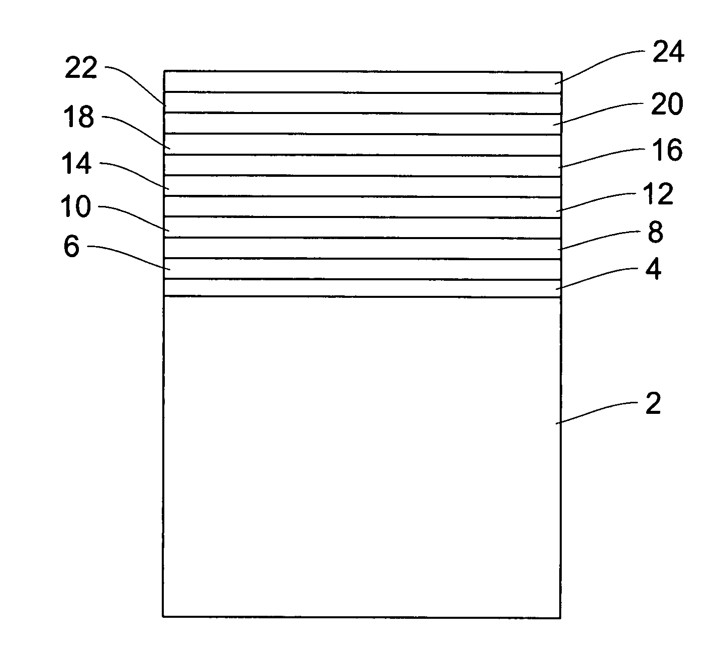
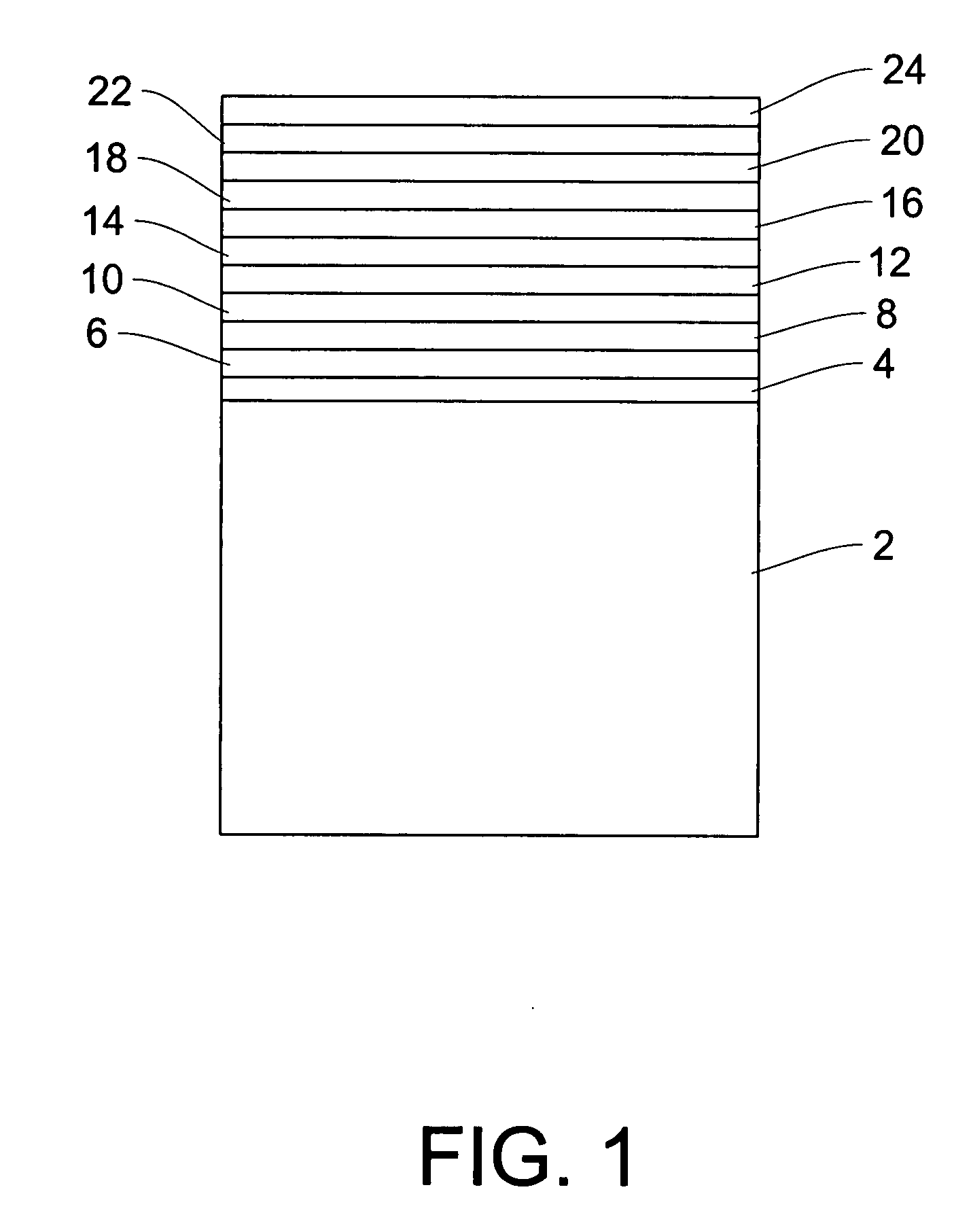
[0019]FIG. 1 is a schematic diagram of the cross-sectional view of a structure of a high power edge emission laser diode in accordance with one embodiment of the present invention. On an n-type substrate 2 is orderly stacked an n-type cladding layer 4, a mode extension layer 6, an n-type cladding layer 8, a first light confinement layer 10, a multi quantum well layer 12, a second light confinement layer 14, a p-type inner cladding layer 16, an etching stop layer 18, a p-type outer cladding layer 20, a barrier reducing layer 22 and a p-type barrier reducing layer 24, wherein the mode extension layer 6 includes plural mode extension sublayers (not shown in the figure). The refraction index of each mode extension sublayer is higher than that of the n-type cladding layer 8 and the refraction index of mode extension sublayers has a chirp periodic distribution. A period is defined as the distance between any two of the contact mode extension sublayers, wherein the mode extension sublayers...


PUM


Abstract

A structure of high power edge emission laser diode that has plural mode extension sublayers with a chirp periodic distribution is provided. The Near Field Pattern (NFP) is an L shape, and the high intensity portion is nicely overlapped with the multi quantum wells. Furthermore, the low intensity portion will extend to the n-type cladding as it can as possible. Accordingly, the optical power density on the mirror surface of the high power edge emission laser diode is lower down and the vertical divergence angle is decreased, so as to prolong its lifetime.

Description

BACKGROUND OF THE INVENTION[0001]1. Field of the Invention[0002]The present invention relates to a structure of a laser diode. More particularly, the present invention relates to a structure of a high power edge emission laser diode.[0003]2. Description of the Prior Art[0004]During the recent years, the society and economy are highly developed and the technology advances in many aspects of people's daily life, the Laser Diode (LD) is a key component for the optical storage, optical communication and medical laser. Because the market of low power LD applied for the optical storage reader is saturated gradually, the specification of LD goes toward the high power applications such as a rewritable optical storage reader, a communication pump LD with a wavelength of 980 nm, a green light pump LD with a wavelength of 808 nm, a full-color laser projector and a full-color projection television (TV) using the high power LD, which all of the aforementioned high power LDs need to have small si...

Claims


Application Information

Patent Timeline
Patent Type & Authority Applications(United States)
IPC IPC(8): H01S5/34H01S5/343
CPCB82Y20/00H01S5/20H01S2301/18H01S5/3213H01S5/343H01S5/2004
Inventor LU, TIEN-CHANGCHEN, CHYONG-HUA
Owner NAT CHIAO TUNG UNIV
Why Eureka
Try Eureka