System and method for automatic layout of integrated circuit

a technology of integrated circuits and layout methods, applied in the field of automatic layout of cell-based ics, can solve the problems of reducing the product performance of semiconductor chips, conventional automatic layout techniques based on such cells cannot achieve automatic layout, and the distance between diffusion layers of different cells within a cell-based ic is not reduced, so as to reduce the variation in the drive characteristics of transistors integrated within cells, reduce the effect of optimal adjustment of the distance between diffusion layers and stress reduction

Inactive Publication Date: 2009-01-15
RENESAS ELECTRONICS CORP
View PDF7 Cites 8 Cited by
  • Summary
  • Abstract
  • Description
  • Claims
  • Application Information

AI Technical Summary

Benefits of technology

[0015]The automatic layout apparatus thus constructed provides optimal adjustment of the distance between diffusion layers for adjacent cells, and thereby effectively reduces the variations in the stress caused by element isolation regions. This effectively reduces the variations in the drive characteristics of transistors integrated within cells.

Problems solved by technology

Therefore, the drive characteristics of the MOS transistors within the cells 101 to 104 exhibit variations, and this results in degradation of the product performance of the semiconductor chip 100.
In recent years, the characteristic variation of the MOS transistor resulting from the variation in the stress as described above is regarded as an issue in connection with the progress in the fine processing technology of the semiconductor circuit.
These techniques, however, do not reduce the variation in the distance between the diffusion layers of the different cells within a cell-based IC.
Therefore, conventional automatic layout techniques based on such cells can not achieve automatic layout based on coordinates of diffusion layers in the gate length direction.
Conventional automatic layout techniques do not sufficiently suppress variations in the MOS transistor characteristics resulting especially from the variations in the stress exerted to the diffusion layer in the gate width direction.

Method used


Image

  • System and method for automatic layout of integrated circuit
  • System and method for automatic layout of integrated circuit
  • System and method for automatic layout of integrated circuit

Examples


Embodiment Construction

[0025]The invention will be now described herein with reference to illustrative embodiments. Those skilled in the art will recognize that many alternative embodiments can be accomplished using the teachings of the present invention and that the invention is not limited to the embodiments illustrated for explanatory purposes. In the following, a description will be given taking an automatic layout apparatus for designing cell-based ICs as one example.

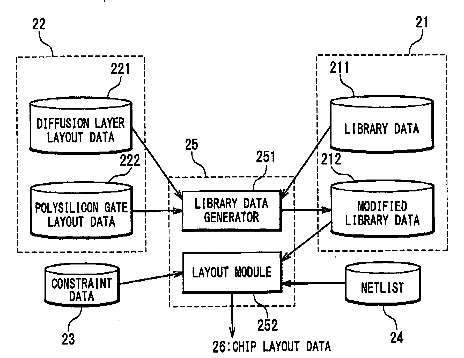
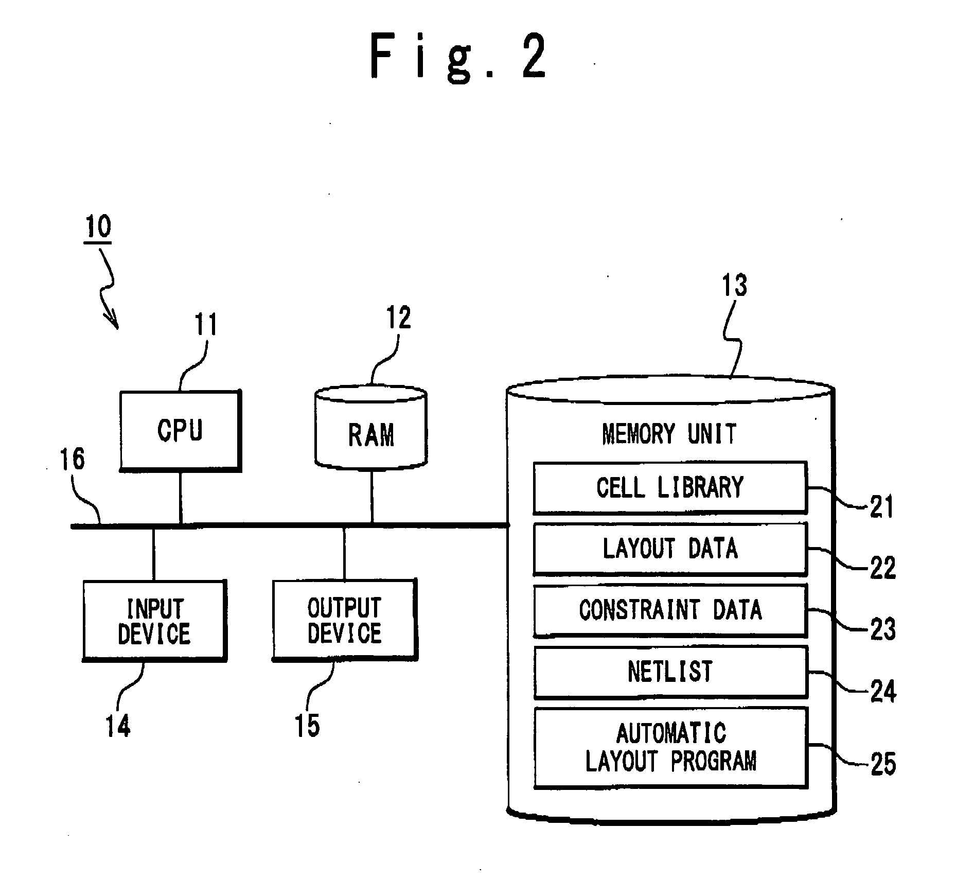
[0026]As shown in FIG. 2, an automatic layout apparatus 10 is provided with a CPU 11, a RAM 12, a storage device 13, an input device 14, and an output device 15, all of which are mutually connected through a bus 16. The storage device 13 is an external storage, such as a hard disk drive. The input device 14 provides various data for the CPU 11 and the storage device 13 in response to user operations. The input device 14 may include a keyboard, a mouse, or the like. The output device 15 visually outputs the layout result of the target cel...


PUM


Abstract

An automatic layout apparatus is provided with: a storage device storing a cell library containing therein cell library data; and a layout tool obtaining from the cell library the cell library data associated with cells to be placed as described in a netlist to perform automatic placement of the cells to be placed. The obtained cell library data include layout coordinates of diffusion layers within the cells to be placed. The layout tool determines positions of the cells to be placed, referring to the layout coordinates of the diffusion layers.

Description

[0001]This application claims the benefit of priority based on Japanese Patent Application No. 2007-184264, filed on Jul. 13, 2007, the disclosure of which is incorporated herein by reference.BACKGROUND OF THE INVENTION [0002]1. Field of the Invention[0003]The present invention relates to a system and method for automatic layout of semiconductor integrated circuits (ICs), more particularly, to a technique for automatic layout of cell-based ICs.[0004]2. Description of the Related Art[0005]Cell-based ICs (Integrated Circuit) are preferably used in various LSIs, such as ASICs (Application Specific Integrated Circuits), microprocessors required to achieve large scale integration and high performance, and ASSPs (Application Specific Standard Products). The cell-based IC is designed by combining ready-made cells to form a user-specific circuit; the cells are prepared in a cell library provided by a semiconductor manufacturer. The cell library prepares various kinds of cells having various...

Claims


Application Information

Patent Timeline
Patent Type & Authority Applications(United States)
IPC IPC(8): G06F17/50
CPCG06F17/5072G06F30/392
Inventor KOBAYASHI, NAOHIRO
Owner RENESAS ELECTRONICS CORP
Why Eureka
Try Eureka