Multi-junction solar cells and methods and apparatuses for forming the same

a solar cell and multi-junction technology, applied in the field of solar cells, can solve the problems of film solar cells degrading, device stability being less than desired, and thin film solar cells including

Inactive Publication Date: 2009-01-22
APPLIED MATERIALS INC
View PDF99 Cites 73 Cited by
  • Summary
  • Abstract
  • Description
  • Claims
  • Application Information

AI Technical Summary

Benefits of technology

[0011]Embodiments of the present invention may further provide a tandem junction photovoltaic device, comprising a first photovoltaic junction and a second photovoltaic junction, wherein the second photovoltaic junction comprises a p-doped microcrystalline silicon layer, an intrinsic type microcrystalline silicon layer, wherein the intrinsic type microcrystalline silicon layer is formed by a multiple step deposition process, wherein each deposition step has a gas mixture having different hydrogen to silane ratio to form different film crystalline fraction in each deposition step, and an n-doped amorphous silicon layer adjacent to the intrinsic type microcrystalline silicon layer. In one embodiment, the different hydrogen to silane ratio controls the crystalline fraction being formed uniformly across the overall thickness of the intrinsic type microcrystalline silicon layer.

Problems solved by technology

It has been found that the properties of thin-film solar cells degrade over time upon exposure to light, which can cause the device stability to be less than desired.
Problems with current thin film solar cells include low efficiency and high cost.

Method used


Image

  • Multi-junction solar cells and methods and apparatuses for forming the same
  • Multi-junction solar cells and methods and apparatuses for forming the same
  • Multi-junction solar cells and methods and apparatuses for forming the same

Examples


examples

[0081]The examples disclosed herein are exemplary in nature and are not meant to limit the scope of the invention unless explicitly set forth in the claims.

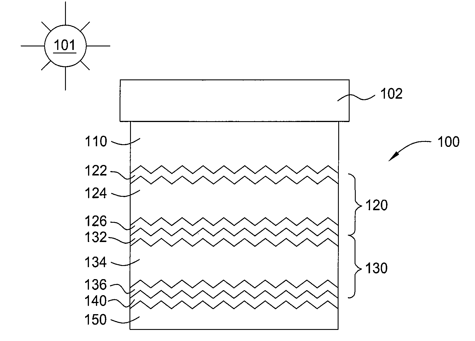
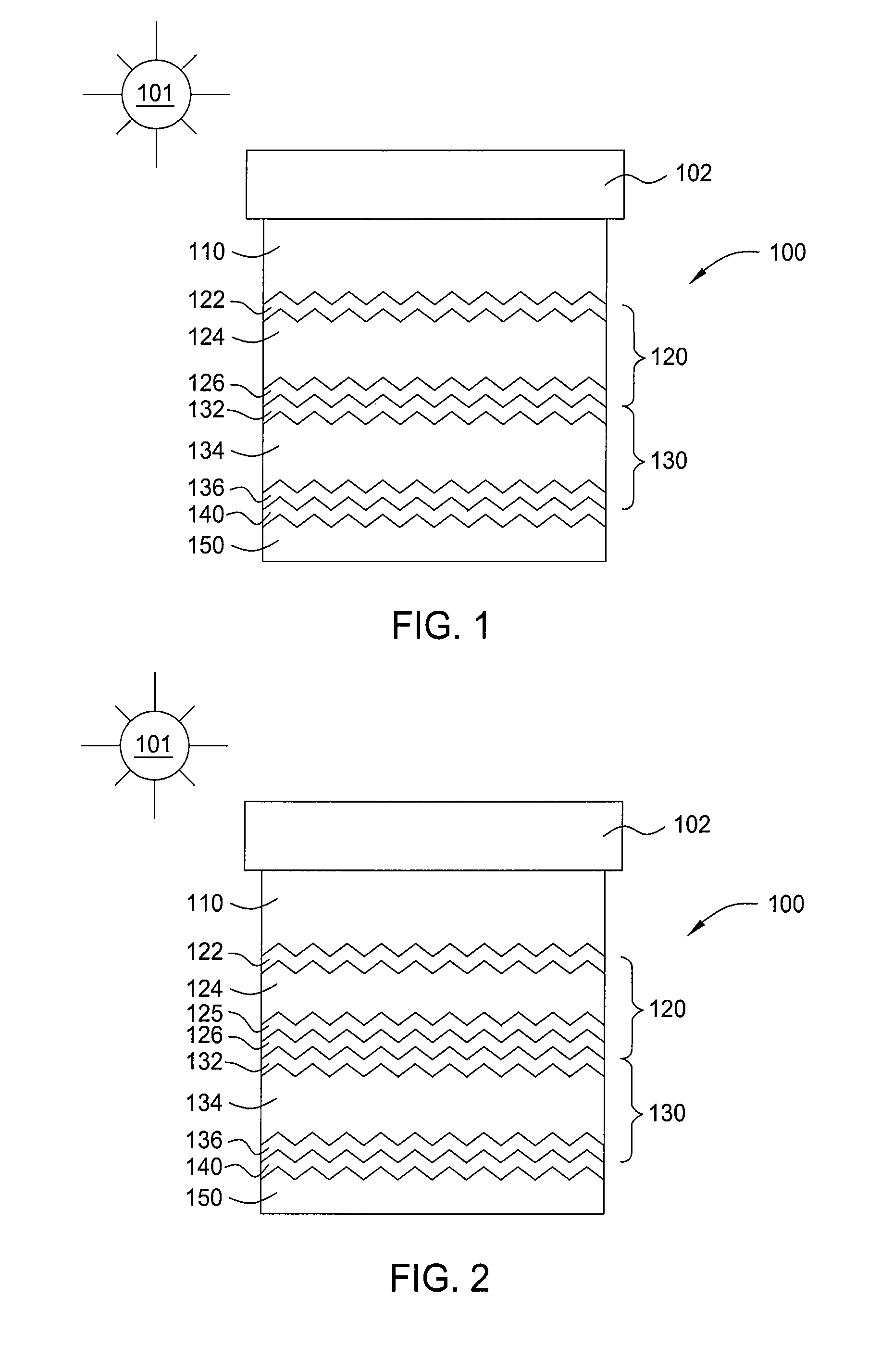
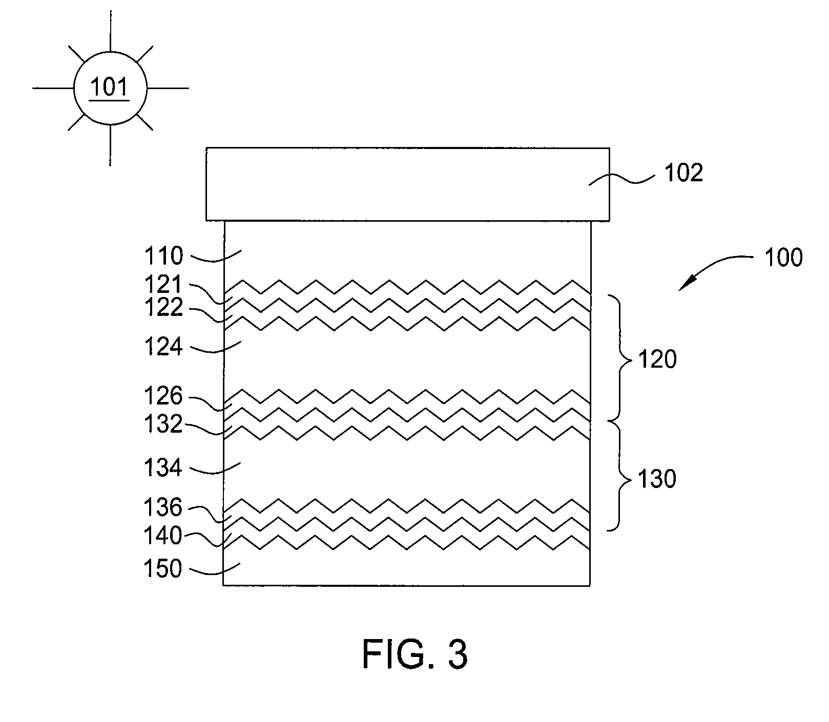
[0082]Substrates having a surface area of 4,320 cm2 were processed in an AKT 4300 PECVD System, available from AKT America, Inc., of Santa Clara, Calif., having an interior chamber volume of 130 liters. Layer 1 was deposited in a first chamber of the PECVD system. Layers 2-4 were deposited in a second chamber of the PECVD system. Layer 5 was deposited in a third chamber of the PECVD system. Layers 6-11 were deposited in a fourth chamber of the PECVD system. The spacing during deposition of layers 1-11 was set to 550 mil and the temperature of the substrate support was set to 200° C. The deposition parameters are set forth in the FIG. 6 to form a tandem p-i-n junction solar cell. Phosphine was provided in a 0.5% mixture in a hydrogen carrier gas. Trimethylboron was provided in a 0.5% mixture in a hydrogen carrier gas. The hydrogen...


PUM


Abstract

Embodiments of the present invention generally relate to solar cells and methods and apparatuses for forming the same. More particularly, embodiments of the present invention relate to thin film multi-junction solar cells and methods and apparatuses for forming the same. Embodiments of the present invention also include an improved thin film silicon solar cell, and methods and apparatus for forming the same, where one or more of the layers in the solar cell comprises at least one amorphous silicon layer that has improved electrical characteristics and mechanical properties, and is capable of being deposited at rates many times faster than conventional amorphous silicon deposition processes.

Description

CROSS-REFERENCE TO RELATED APPLICATIONS[0001]This application is a continuation-in-part of co-pending U.S. patent application Ser. No. 12 / 110,120 filed Apr. 25, 2008 (Attorney Docket No. APPM / 11709 P2), which is a continuation-in-part application of co-pending U.S. patent application Ser. No. 11 / 671,988 filed Feb. 6, 2007 (Attorney Docket No. APPM / 11709 P1), which is a continuation-in-part application of co-pending U.S. patent application Ser. No. 11 / 624,677, filed Jan. 18, 2007 (Attorney Docket No. APPM / 11709), which are incorporated by reference in their entireties.[0002]This application also claims benefit of U.S. Provisional Patent Application Ser. No. 60 / 951,608, filed Jul. 24, 2007 (Attorney Docket No. APPM / 11711L) and the U.S. Provisional Patent Application Ser. No. 60 / 982,400, filed Oct. 24, 2007 (Attorney Docket No. APPM / 11711L02), both of which are incorporated by reference in their entireties.BACKGROUND OF THE INVENTION[0003]1. Field of the Invention[0004]Embodiments of t...

Claims


Application Information

Patent Timeline
Patent Type & Authority Applications(United States)
IPC IPC(8): H01L31/00H01L21/20
CPCH01L31/03685H01L31/076H01L31/1804Y02E10/547H01L31/1824Y02E10/545Y02E10/548Y02P70/50
Inventor SHENG, SHURANCHAE, YONG KEECHOI, SOO YOUNGWON, TAE KYUNGLI, LIWEI
Owner APPLIED MATERIALS INC
Why Eureka
Try Eureka