

Shallow trench isolation structures for semiconductor devices including doped oxide film liners and methods of manufacturing the same
a technology of semiconductor devices and trench isolation structures, which is applied in the direction of semiconductor devices, semiconductor/solid-state device details, electrical apparatus, etc., can solve the problems of various degradations of semiconductor devices, degrading the electrical characteristics of semiconductor devices, and increasing the difficulty of forming the sti structure for separating semiconductor devices, etc., to achieve high etching resistance
- Summary
- Abstract
- Description
- Claims
- Application Information
AI Technical Summary
Benefits of technology
Problems solved by technology
Method used
Image

Examples
Embodiment Construction
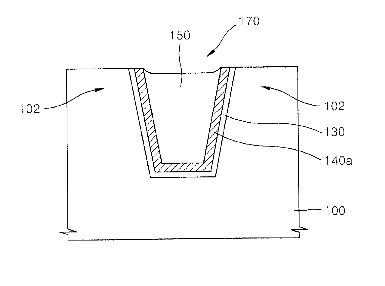
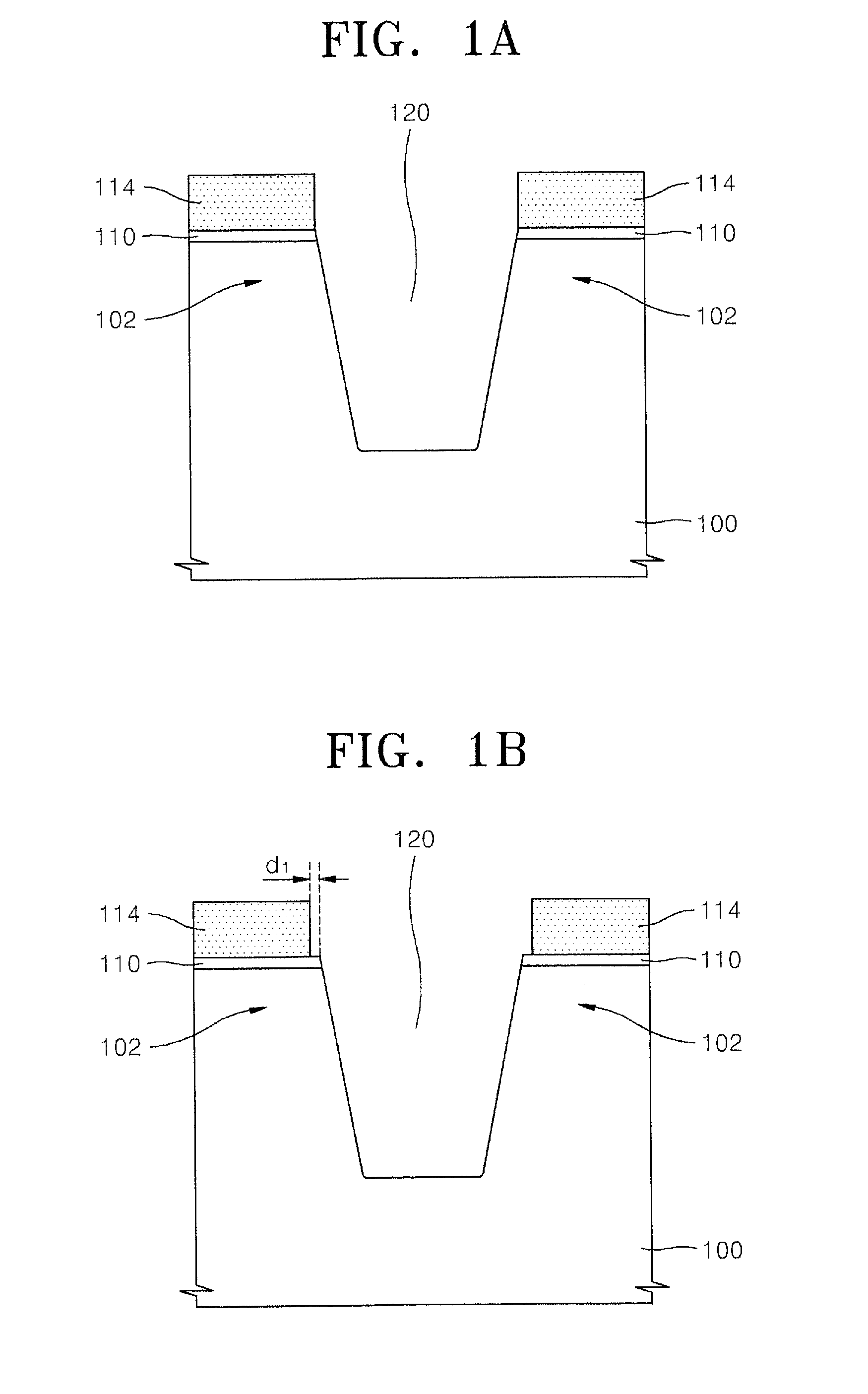
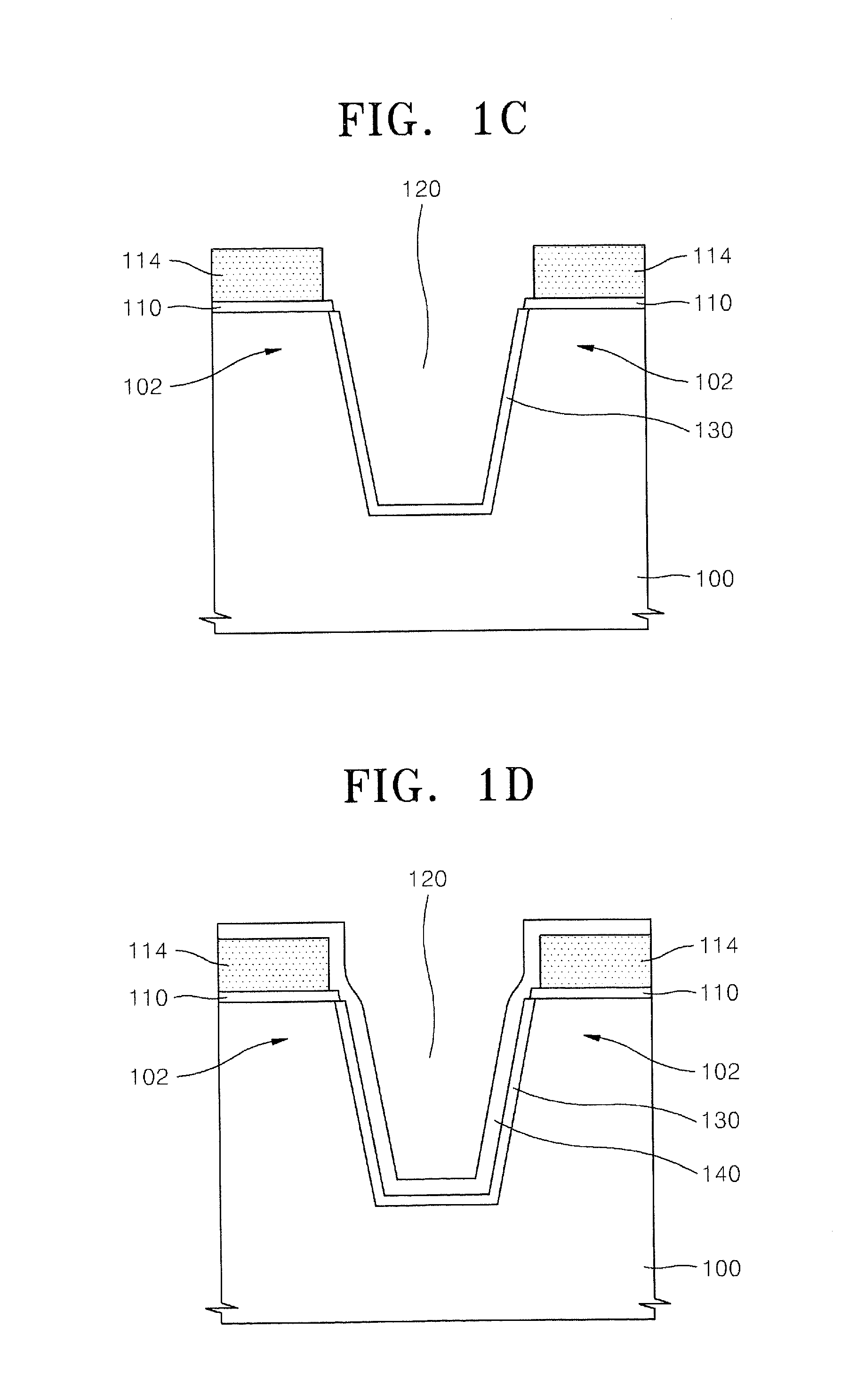
[0015]The present invention is described more fully hereinafter with reference to the accompanying drawings, in which embodiments of the present invention are shown. The present invention may, however, be embodied in many different forms and should not be construed as limited to the embodiments set forth herein. Rather, these embodiments are provided so that this disclosure will be thorough and complete, and will fully convey the scope of the present invention to those skilled in the art. In the drawings, the sizes and relative sizes of layers and regions may be exaggerated for clarity.
[0016]It will be understood that when an element or layer is referred to as being “on,”“connected to” or “coupled to” another element or layer, it can be directly on, connected or coupled to the other element or layer or intervening elements or layers may be present. In contrast, when an element is referred to as being “directly on,”“directly connected to” or “directly coupled to” another element or l...
PUM
 Abstract
Description
Claims
Application Information