Wireless IC device and electronic device

a technology of electronic devices and wires, applied in the field of wireless ic devices, can solve the problems of increasing size and increasing cost, and achieve the effect of easy impedance matching

Active Publication Date: 2009-01-22
MURATA MFG CO LTD
View PDF8 Cites 124 Cited by
  • Summary
  • Abstract
  • Description
  • Claims
  • Application Information

AI Technical Summary

Benefits of technology

[0007]Preferred embodiments of the present invention provide a wireless IC device which does not require a dedicated antenna and hence makes it possible to achieve miniaturization and which also allows easy impedance matching, and an electronic apparatus including the wireless IC device.
[0010]In the wireless IC device according to the first and second preferred embodiments of the present invention, the wireless IC chip or the feeder circuit board and the ground electrode are coupled to each other via the substantially loop-shaped electrode, and the ground electrode functions as a radiator plate (antenna) of the wireless IC chip. That is, the wireless IC chip is operated via the substantially loop-shaped electrode by a signal received by the ground electrode, and a response signal from the wireless IC chip is radiated from the ground electrode to the outside via the substantially loop-shaped electrode. Therefore, it is not necessary to fabricate a dedicated antenna, nor is it necessary to provide a space for installation of that antenna. Further, the substantially loop-shaped electrode can provide impedance matching between the wireless IC chip and the ground electrode, and hence it is unnecessary to provide a separate matching part, thereby improving the efficiency of signal transmission between the wireless IC chip and the ground electrode.
[0011]In the wireless IC device according to the second preferred embodiment of the present invention, the feeder circuit board is interposed between the wireless IC chip and the substantially loop-shaped electrode. This feeder circuit board includes a resonant circuit and / or a matching circuit having an inductance element, and the frequency to be used is set by the resonant circuit and / or the matching circuit. When the wireless IC chip is changed in accordance with the frequency used by the RFID system, it suffices to change only the design of the resonant circuit and / or the matching circuit, and there is no need to change the shape, size, or arrangement of the radiator plate (ground electrode) or the coupling state between the substantially loop-shaped electrode and the ground electrode or the feeder circuit board. Further, the resonant circuit and / or the matching circuit can also include a function of matching the impedance between the wireless IC chip and the ground electrode, thereby making it possible to improve the efficiency of signal transmission between the wireless IC chip and the ground electrode.
[0013]According to a preferred embodiment of the present invention, an existing ground electrode on the circuit board can be used as an antenna, and it is thus unnecessary to arrange an antenna as a separate component, thereby achieving miniaturization of the wireless IC device or the apparatus with the wireless IC device installed. Further, an impedance matching function can be imparted to the resonant circuit and / or the matching circuit included in the substantially loop-shaped electrode and / or the feeder circuit board, thus eliminating the need to separately provide a matching part.

Problems solved by technology

However, since this RFID tag includes a dedicated antenna, an antenna fabrication process is required, leading to an increase in cost.
Further, an installation space for the antenna is also required, resulting in an increase in size.

Method used


Image

  • Wireless IC device and electronic device
  • Wireless IC device and electronic device
  • Wireless IC device and electronic device

Examples


first preferred embodiment

FIGS. 1A and 1B and FIG. 2

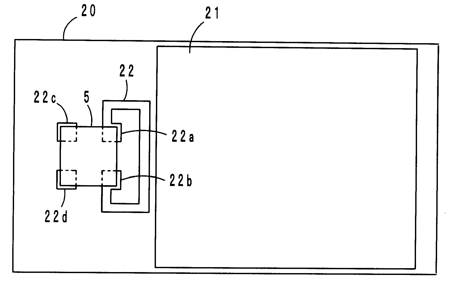
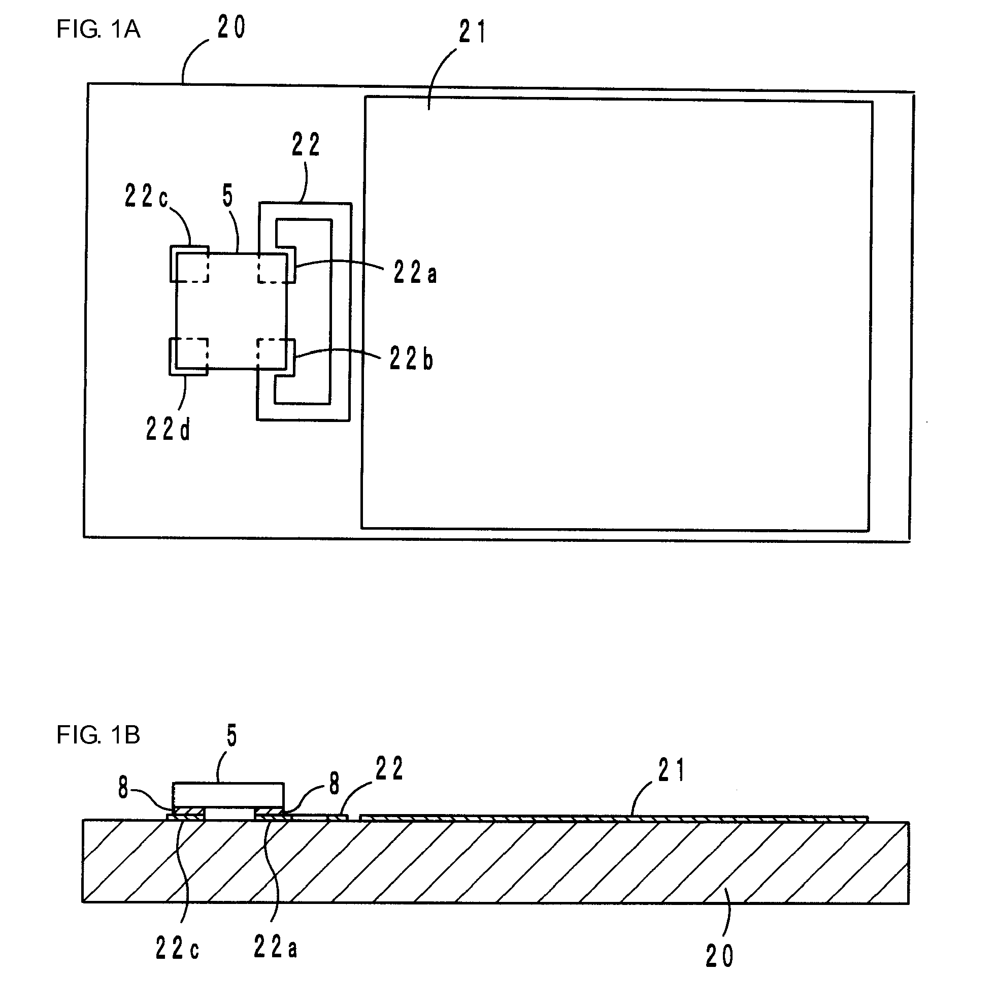
[0029]FIGS. 1A and 1B show a wireless IC device according to a first preferred embodiment of the present invention. This wireless IC device includes a wireless IC chip 5 for processing a transmission / reception signal of a predetermined frequency, a printed wiring circuit board 20 on which the wireless IC chip 5 is mounted, and a ground electrode 21 and a substantially loop-shaped electrode 22 that are disposed on the circuit board 20. The ground electrode 21 and the substantially loop-shaped electrode 22 are provided on the principal surface of the printed wiring circuit board 20 through application of a conductive paste, etching of a metal foil provided on the circuit board 20, or the like.

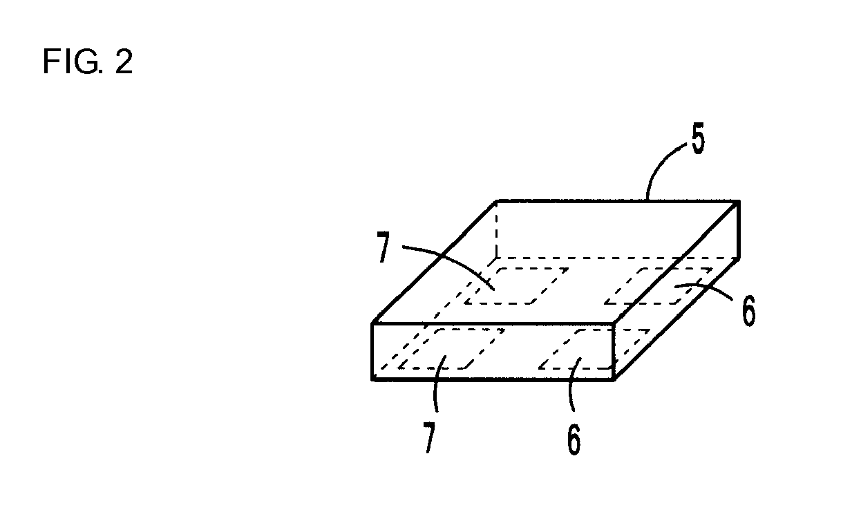
[0030]The wireless IC chip 5 preferably includes a clock circuit, a logic circuit, a memory circuit, and the like, and stores necessary information. As shown in FIG. 2, the wireless IC chip 5 has input / output terminal electrodes 6, 6 and mounting terminal electrodes 7, 7...

second preferred embodiment

FIGS. 3A and 3B

[0035]FIGS. 3A and 3B show a wireless IC device according to a second preferred embodiment of the present invention. This wireless IC device is of basically the same configuration as that of the above-mentioned first preferred embodiment, except that the ground electrode 21 and the substantially loop-shaped electrode 22 are disposed on the back surface of the printed wiring circuit board 20. Connection electrodes 24a to 24d are disposed on the front surface of the circuit board 20. The connection electrodes 24a, 24b are electrically connected to the opposite ends of the substantially loop-shaped electrode 22 via a via-hole conductor 23. The connection electrodes 24a to 24d correspond to the connection electrodes 22a to 22d shown in FIGS. 1A and 1B, and are electrically connected to the terminal electrodes 6, 6, 7, 7 (see FIG. 2) of the wireless IC chip 5 via the metal bump 8.

[0036]The coupling state between the ground electrode 21 and the substantially loop-shaped ele...

third preferred embodiment

FIGS. 4A to 4C

[0037]FIGS. 4A to 4C show a wireless IC device according to a third preferred embodiment of the present invention. In this wireless IC device, a substantially loop-shaped electrode 25 is defined by connection electrodes 25a, 25b provided on the front surface of the printed wiring circuit board 20, via-hole conductors 28, 28, and an internal electrode 29. The substantially loop-shaped electrode 25 is coupled by an electric field to the ground electrode 21 provided on the back surface of the circuit board 20. The connection electrodes 25a, 25b and the connection electrodes 25c, 25d are electrically connected to the terminal electrodes 6, 6, 7, 7 (see FIG. 2) of the wireless IC chip 5 via the metal bump 8.

[0038]The substantially loop-shaped electrode 25 is arranged substantially perpendicular and in close proximity to the ground electrode 21, and the two electrodes are coupled to each other by an electric field. That is, the substantially loop-shaped electrode 25 produces...


PUM


Abstract

A wireless IC device includes a wireless IC chip for processing a transmission / reception signal, a printed wiring circuit board on which the wireless IC chip is mounted, a ground electrode disposed on the circuit board, and a substantially loop-shaped electrode that is electrically conducted to the wireless IC chip and disposed on the circuit board so as to be coupled to the ground electrode by an electromagnetic field. The ground electrode is coupled to the wireless IC chip via the substantially loop-shaped electrode to transmit / receive a radio frequency signal. A feeder circuit board including a resonant circuit and / or a matching circuit may be interposed between the wireless IC chip and the substantially loop-shaped electrode.

Description

BACKGROUND OF THE INVENTION[0001]1. Field of the Invention[0002]The present invention relates to a wireless IC device, and more specifically to a wireless IC device having a wireless IC chip used in an RFID (Radio Frequency Identification) system, and an electronic apparatus including the wireless IC device.[0003]2. Description of the Related Art[0004]In recent years, an RFID system has been developed as an item management system, in which communication is performed in a non-contact manner between a reader / writer that generates an induction field, and an IC chip (also referred to as the IC tag or wireless IC chip) storing predetermined information and attached to an item, a container, or the like to thereby transmit information.[0005]PCT Japanese Translation Patent Publication No. 11-515094 describes an RFID tag including an IC chip and an antenna formed within a printed wiring circuit board. In this RFID tag, the antenna within the printed wiring circuit board and the IC chip mount...

Claims


Application Information

Patent Timeline
Patent Type & Authority Applications(United States)
IPC IPC(8): H01Q7/00H01Q1/50
CPCG06K19/07749G06K19/0775H01Q1/2225H01Q1/38H01Q7/00H01L2224/16225H05K1/0243H05K1/141H05K1/16H05K2201/10098H01L2224/16227H05K1/0239H01Q1/44G06K19/07H01Q1/50
Inventor KATAYA, TAKESHIKATO, NOBORUISHINO, SATOSHIIKEMOTO, NOBUOKIMURA, IKUHEI
Owner MURATA MFG CO LTD
Why Eureka
Try Eureka