

Semiconductor device
a semiconductor device and device technology, applied in the field of semiconductor devices, can solve the problems of inability to specify, inability to meet the timing constraint (setup violation), and inability to specify the number of pins of the semiconductor devi
- Summary
- Abstract
- Description
- Claims
- Application Information
AI Technical Summary
Benefits of technology
Problems solved by technology
Method used
Image

Examples
first embodiment
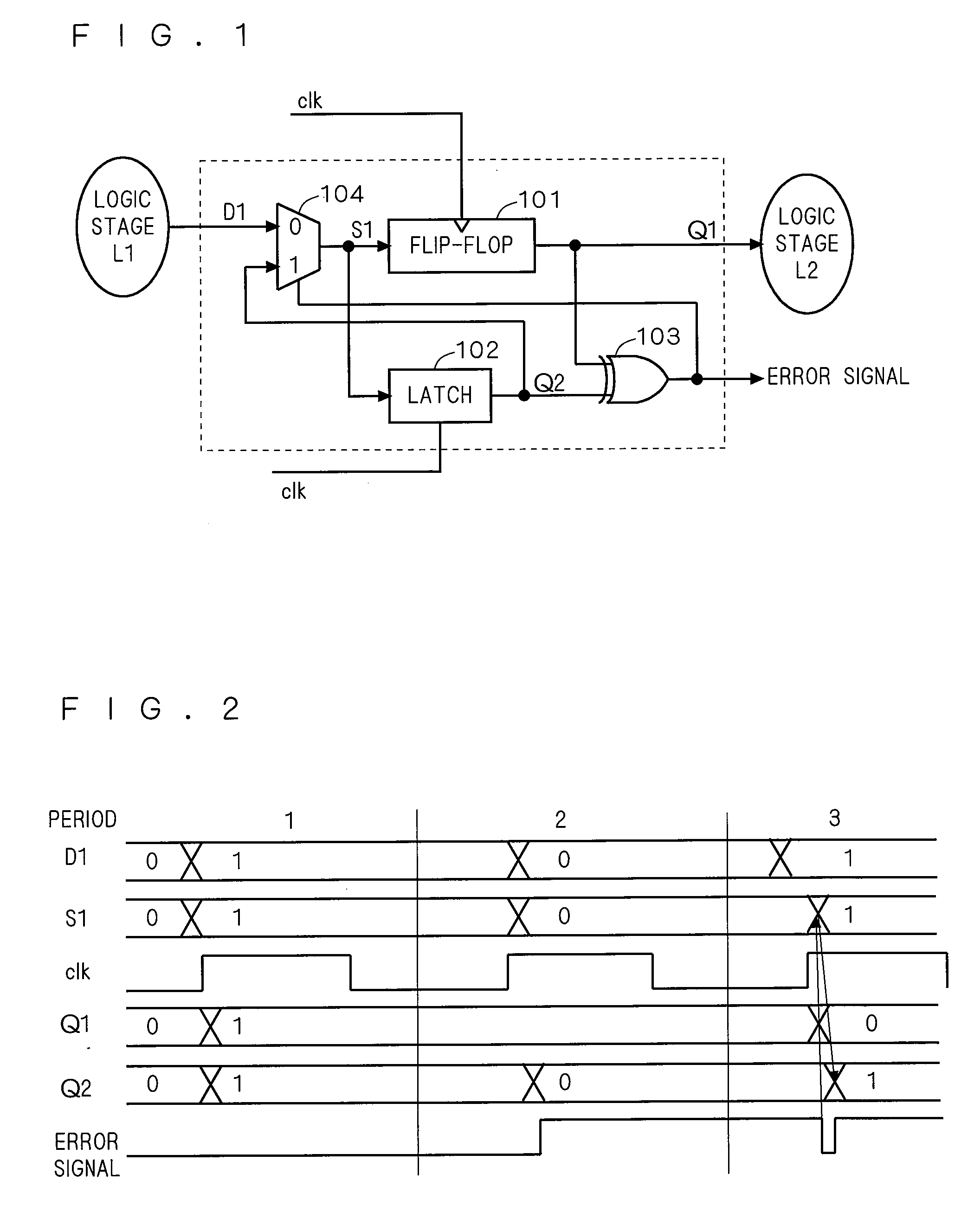
[0050]Before describing a semiconductor device of the present invention, a configuration and a drive of a Razor circuit disclosed in Dan Ernest, et al., “Razor: Low-Power Pipeline Based on Circuit-Level Timing Speculation”, IEEE MICRO, 2004, pp. 10-20 is described. FIG. 1 shows a circuit diagram of the Razor circuit, and FIG. 2 shows a timing chart of the Razor circuit.
[0051]The Razor circuit shown in FIG. 1 is provided with a flip-flop circuit 101 for capturing a data signal in synchronization with a rising edge of a clock signal clk, and a latch circuit 102 for capturing the data signal during a High period of the clock signal clk. Further, the Razor circuit shown in FIG. 1 is provided with a comparator 103 for comparing an output Q1 of the flip-flop circuit 101 and an output Q2 of the latch circuit 102, and a selector circuit 104 for switching a data signal D1 output from a logic stage L1, which is a logic circuit, and a data signal Q2 output from the latch circuit 102, depending...
second embodiment
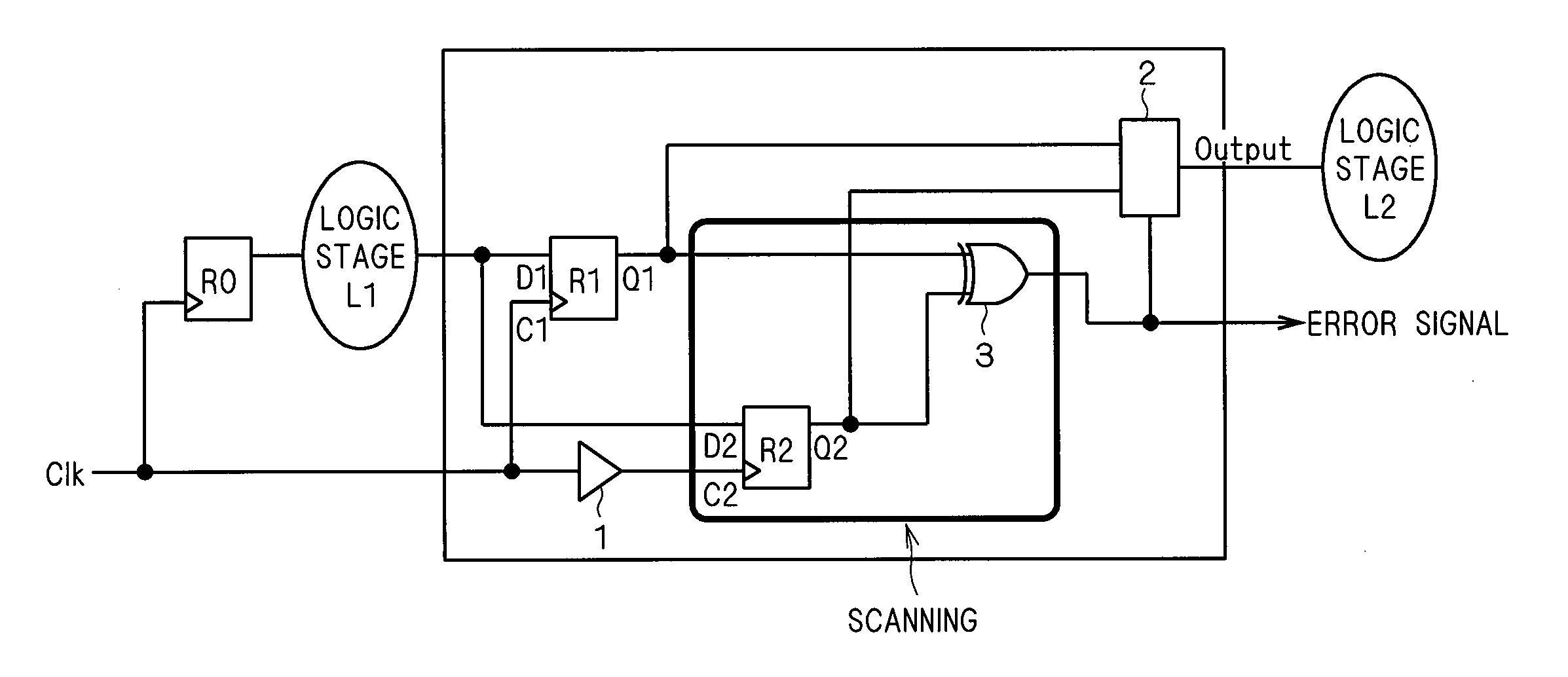
[0079]A circuit shown in FIG. 8 makes a path from a register R0 through the logic stage L1 to the register R1 a critical path and transmits the data signal Q1 output from the register R1 to a logic of a subsequent stage (logic stage L2). Herein, in the circuit shown in FIG. 8, the clock signal C1 to be supplied to the register R1 is not the clock signal Clk directly supplied from outside but a gated clock signal obtained by figuring out a logical sum with an Enable signal in an AND circuit 20, which serves as the clock control means. Meanwhile, the clock control means is not limited to the AND circuit and any circuit provided with an equivalent function may be used.
[0080]Also, in the circuit shown in FIG. 8, the register R2 in which the setup violation condition is eased by inserting a buffer B2 into the clock line is provided, and the comparator 3 compares the output result of the same with that of the register R1. Further, in the circuit shown in FIG. 8, when the Enable signal is ...
third embodiment
[0095]In the second embodiment, it is possible to detect the setup violation of the data signal and the setup violation of the Enable signal, respectively; however, in a case in which the setup violation of the data signal and that of the Enable signal occur in the same period, it has not been possible to detect the setup violation. Therefore, in this embodiment, the setup violation of the data signal and that of the Enable signal generated in the same period may be detected by using the circuit shown in FIG. 12.
[0096]In general, the Enable signal is often used to control a bus (a plurality of bits), so that in the circuit shown in FIG. 12, a circuit for detecting only the Enable signal is newly added to a circuit group in which the setup violation of the Enable signal is controlled by the same Enable signal. That is to say, the circuit shown in FIG. 12 is composed of circuits A1 to A3 provided with the registers R1 and R2 and the comparator 3 for detecting the setup violation of th...
PUM
 Abstract
Description
Claims
Application Information