Plasma processing apparatus and method of plasma distribution correction
a technology of plasma distribution and processing apparatus, which is applied in the direction of instruments, fluid pressure measurement, coatings, etc., can solve the problems of complicated configuration of the apparatus, and achieve the effect of simplifying the apparatus configuration
- Summary
- Abstract
- Description
- Claims
- Application Information
AI Technical Summary
Benefits of technology
Problems solved by technology
Method used
Image
Examples
first embodiment
[0049]First, an explanation will be made of a plasma processing apparatus in accordance with the present invention.
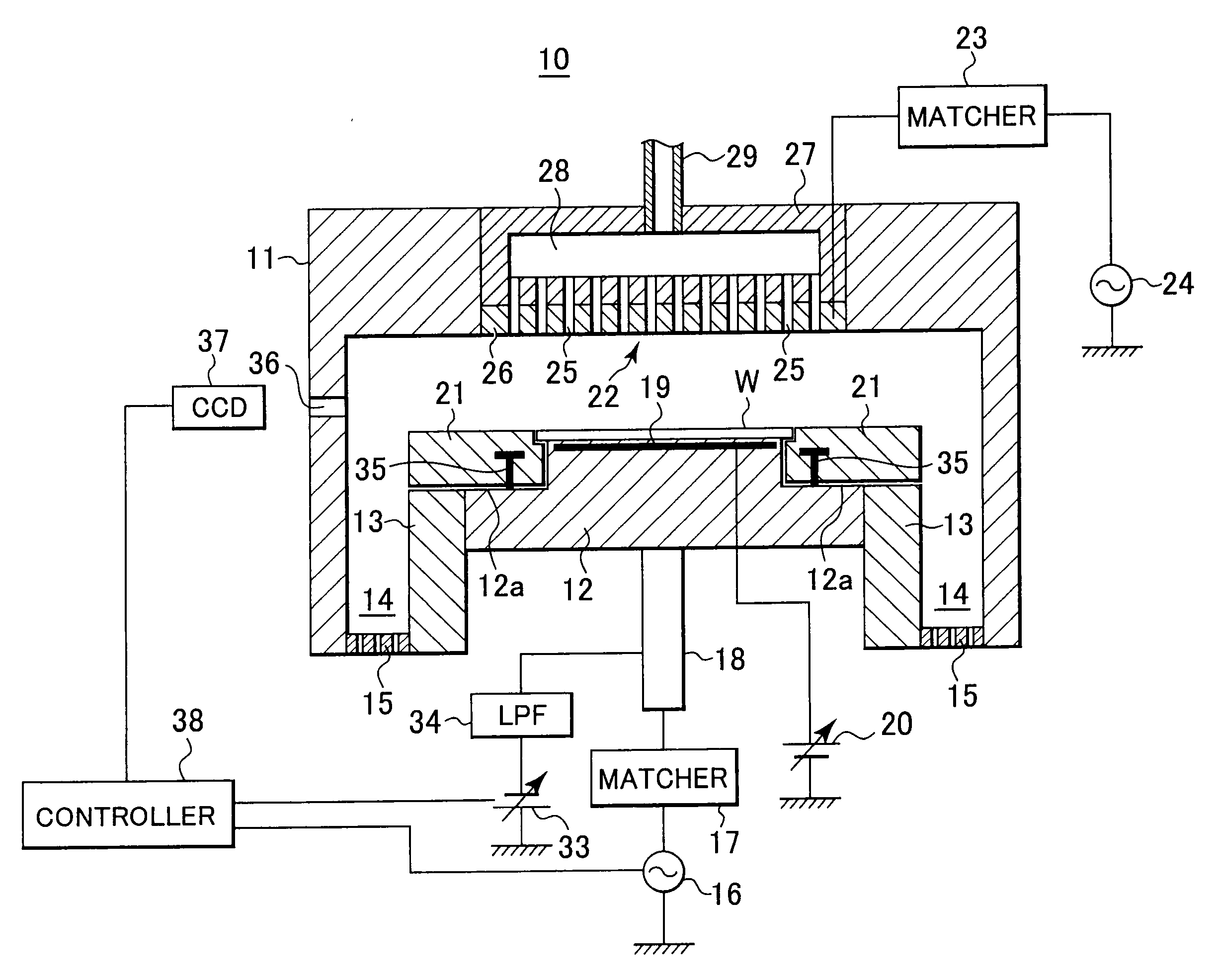
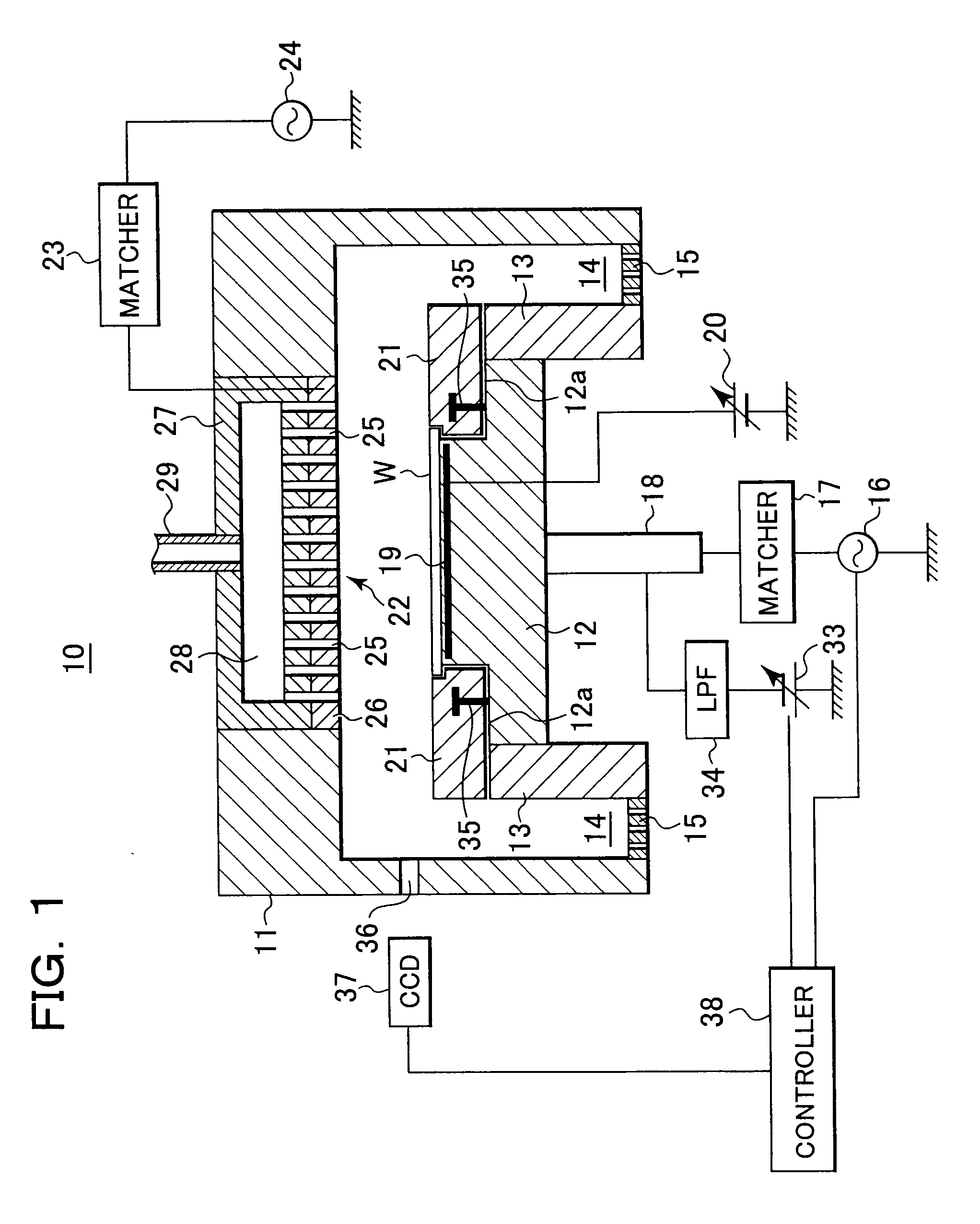
[0050]FIG. 1 is a cross-sectional view schematically illustrating the configuration of a plasma processing apparatus in accordance with a first embodiment of the present invention. This plasma processing apparatus is configured to perform an etching processing on a semiconductor wafer serving as a substrate.
[0051]In FIG. 1, a plasma processing apparatus 10 is provided with a chamber 11 (housing chamber) for housing semiconductor wafers (hereinafter simply referred to as “wafers”) W having a diameter of, for example, 300 mm, and an electrostatic chuck 12 (mounting stage) to be mounted with a wafer W is disposed within the chamber 11. The electrostatic chuck 12 is formed of a lower disc-shaped member having a specific diameter on which there is placed an upper disc-shaped member having a diameter smaller than the diameter of the lower disc-shaped member. Note that the ele...
second embodiment
[0084]Next, an explanation will be made of a plasma processing apparatus in accordance with the present invention.
[0085]The present embodiment is basically the same in configuration and effect as the above-described first embodiment and only differs in the way the amount of wear in a focus ring is measured. The same parts of configuration and effect, therefore, will not be explained further and only the different parts thereof will be explained hereinafter.
[0086]FIG. 6 is a cross-sectional view schematically illustrating the configuration of a plasma processing apparatus in accordance with the present embodiment.
[0087]In FIG. 6, a plasma processing apparatus 40 is provided with a focus ring wear measurement unit 41. The focus ring wear measurement unit 41 is provided with a laser light oscillator 42 for irradiating infrared low-coherent light as laser light (for example, SLD having a wavelength of 1300 nm), a 2×2 coupler 44 connected through the laser light oscillator 42 and an opti...
third embodiment
[0104]Next, an explanation will be made of a plasma processing apparatus in accordance with the present invention.
[0105]The present embodiment is basically the same in configuration and effect as the above-described first embodiment and only differs in the way the amount of wear in a focus ring is predicted. The same parts of configuration and effect, therefore, will not be explained further and only the different parts thereof will be explained hereinafter.
[0106]FIG. 8 is a cross-sectional view schematically illustrating the configuration of a plasma processing apparatus in accordance with the present embodiment.
[0107]In FIG. 8, a plasma processing apparatus 50 is provided with a sensor 51 provided on the side wall of a chamber 11 and a controller 52 (control unit) connected to the sensor 51. The sensor 51 measures a pressure and a temperature (plasma processing conditions) within the chamber 11 and transmits the result of measurement to the controller 52.
[0108]The controller 52 is...
PUM
| Property | Measurement | Unit |
|---|---|---|
| diameter | aaaaa | aaaaa |
| DC voltage | aaaaa | aaaaa |
| DC voltage | aaaaa | aaaaa |
Abstract
Description
Claims
Application Information


