Organic light emitting display and method of manufacturing the same

a technology of light-emitting display and organic material, which is applied in the manufacture of electric discharge tubes/lamps, discharge tubes luminescnet screens, electrode systems, etc., can solve the problems of limited effectiveness in preventing (or reducing) damage generated during the use of organic light-emitting displays

Active Publication Date: 2009-01-29
SAMSUNG DISPLAY CO LTD
View PDF2 Cites 66 Cited by
  • Summary
  • Abstract
  • Description
  • Claims
  • Application Information

AI Technical Summary

Benefits of technology

[0011]Other aspects of the present invention are directed toward an organic light emitting display capable of preventing (or reducing) damage caused by the ESD without adding an additional protecting element (or an ESD protecting circuit) and a method of manufacturing the same.

Problems solved by technology

When the ESD is received, the channels and the gate insulating layers of the TFTs may be damaged, erroneous operations may be generated by the short between the gate electrodes and wiring lines, and / or the driving circuit may be damaged due to the electric influence.
However, the element or the protecting circuit is designed to discharge the ESD generated during the manufacturing processes and its effectiveness in preventing (or reducing) the damage generated during the use of the organic light emitting display is limited.

Method used


Image

  • Organic light emitting display and method of manufacturing the same
  • Organic light emitting display and method of manufacturing the same
  • Organic light emitting display and method of manufacturing the same

Examples


first embodiment

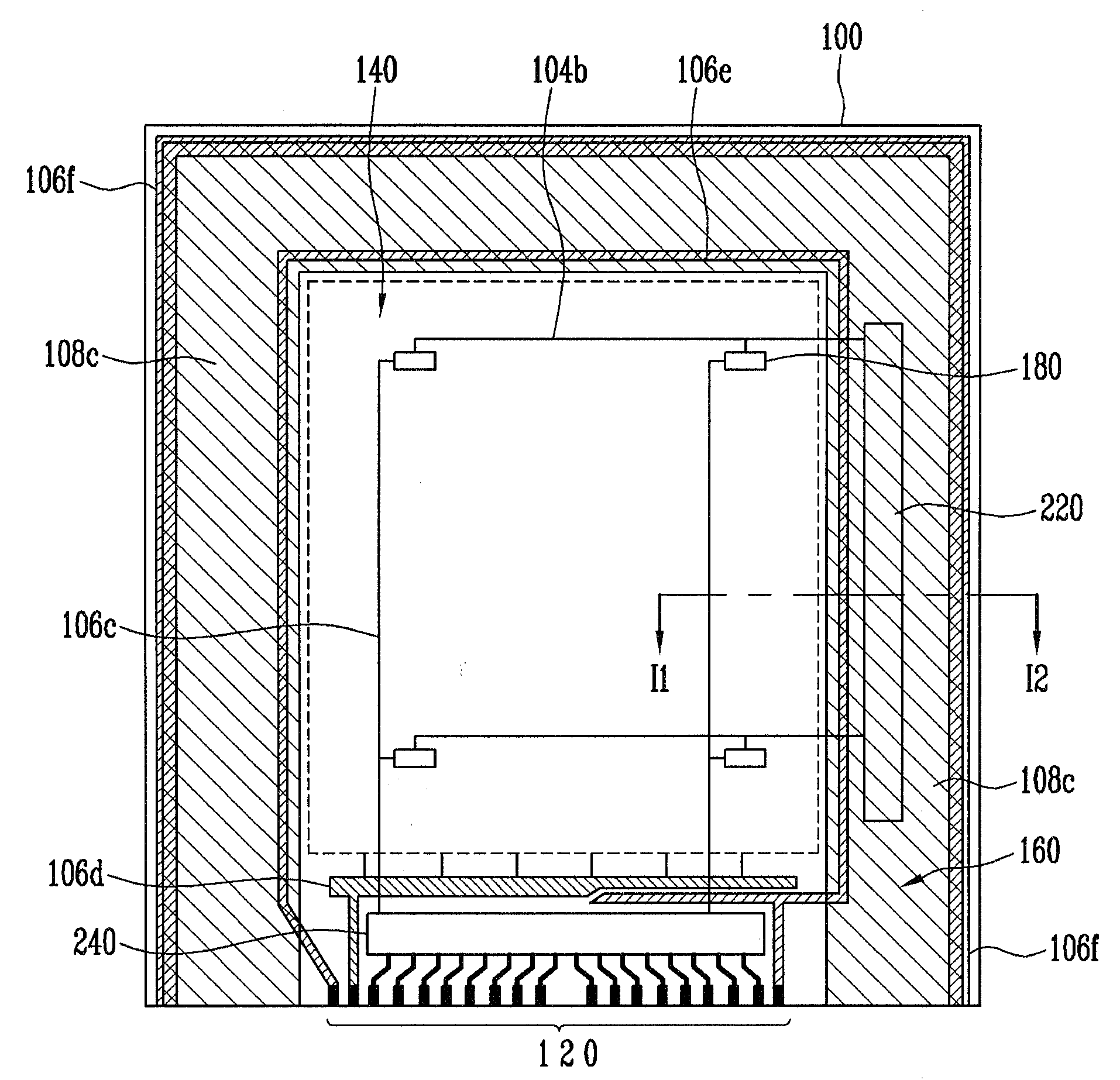
[0033]FIG. 4 is a sectional view schematically illustrating an organic light emitting display according to the present invention and is a sectional view taken along the I1-I2 of FIG. 1.

[0034]A buffer layer 101 is formed on the substrate 100 in both the pixel region 140 and the non-pixel region 160. A semiconductor layer 102 that provides an active layer is formed on the buffer layer 101. The semiconductor layer 102 formed in the pixel region 140 provides the active layer of a TFT for driving the OLED 180, and the semiconductor layer 102 formed in the non-pixel region 160 provides the active layer of a TFT that constitutes the driving circuit unit.

[0035]The gate insulating layer 103 is formed in the pixel region 140 and the non-pixel region 160 and on the semiconductor layer 102, and the gate electrode 104a is formed on the gate insulating layer 103 on the semiconductor layer 102. Here, the scan line 104b coupled to the gate electrode 104a is formed in the pixel region 140, and the s...

second embodiment

[0039]FIG. 5 is a sectional view schematically illustrating an organic light emitting display according to the present invention and is a sectional view taken along the line I1-I2 of FIG. 1.

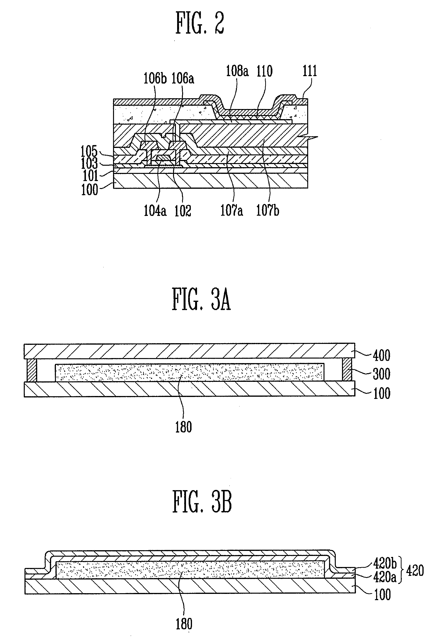
[0040]The organic light emitting display according to the second embodiment of the present invention has substantially the same structure as the organic light emitting display according to the first embodiment. However, the light shielding layer 108c of the non-pixel region 160 is covered with a protecting layer 109 formed of an organic layer.

[0041]As described in the first embodiment, when the shielding layer 108c is formed on the planarizing layer 107b formed of acryl, the attachment state between the planarizing layer 107b and the shielding layer 108c may deteriorate due to the weak layer structure of acryl. Therefore, the shielding layer 108c is covered with the protecting layer 109 so that the attachment state between the planarizing layer 107b and the shielding layer 108c can be maintained ...

third embodiment

[0043]FIG. 6 is a sectional view schematically illustrating an organic light emitting display according to the present invention and is taken along the line I1-I2 of FIG. 1.

[0044]The organic light emitting display according to the third embodiment of the present invention has substantially the same structure as the structure of the organic light emitting display according to the first embodiment. However, the cathode electrode 111 is extended to the top of the shielding layer 108c (or is extended to be on the shielding layer 108c). Here, the pixel defining layer 109 can reside between the cathode electrode 111 and the shielding layer 108c in the remaining part excluding the contacting part between the cathode electrode 111 and the shielding layer 108c.

[0045]The cathode electrode 111 is extended to the top of the shielding layer 108c (or is extended to be on the shielding layer 108c) to form an electric contact in the overlapping part between the cathode electrode 111 and the shield...


PUM


Abstract

An organic light emitting display and a method of manufacturing the same. The light emitting display includes a substrate having a pixel region and a non-pixel region; an organic light emitting diode (OLED) in the pixel region and including a first electrode, an organic thin layer, and a second electrode; a driving circuit unit in the non-pixel region and for driving the OLED; a shielding layer in the non-pixel region and on the driving circuit unit, the shielding layer being electrically coupled to a ground power source; and an insulating layer interposed between the driving circuit unit and the shielding layer. The shielding layer effectively protects the driving circuit unit in the non-pixel region form electrostatic discharge (ESD). Also, the light emitting display may include a guard ring at an edge portion of the non-pixel region and electrically coupled to the shielding layer to further protect the driving circuit from ESD.

Description

CROSS-REFERENCE TO RELATED APPLICATIONS[0001]This application claims priority to and the benefit of Korean Patent Application No. 10-2007-0073385, filed on Jul. 23, 2007, in the Korean Intellectual Property Office, the entire content of which is incorporated herein by reference.BACKGROUND[0002]1. Field of the Invention[0003]The present invention relates to an organic light emitting display and a method of manufacturing the same, and, more particularly to, an organic light emitting display capable of protecting a driving circuit from electrostatic discharge (ESD) and a method of manufacturing the same.[0004]2. Description of the Related Art[0005]An organic light emitting display is a self-emission display that has a wider view angle, a higher contrast, a faster response speed, and a lower power consumption as compared to that of a liquid crystal display (LCD). Because a back light is not required, the organic light emitting display can be made to be light and thin.[0006]The organic l...

Claims


Application Information

Patent Timeline
Patent Type & Authority Applications(United States)
IPC IPC(8): H01J1/62H01J9/00
CPCH01L27/3276H01L27/3272H10K59/126H10K59/131H05B33/22H05B33/26
Inventor KWAK, WON-KYUCHUN, HAE-JIN
Owner SAMSUNG DISPLAY CO LTD
Why Eureka
Try Eureka