Composition and method for selectively etching gate spacer oxide material

a gate spacer oxide and selective etching technology, applied in the direction of electrical equipment, chemistry apparatus and processes, semiconductor devices, etc., can solve the problems of increased parasitic capacitance, device contact resistance, tight tolerance of pattern definition,

Inactive Publication Date: 2009-02-05
ADVANCED TECH MATERIALS INC
View PDF23 Cites 45 Cited by
  • Summary
  • Abstract
  • Description
  • Claims
  • Application Information

AI Technical Summary

Benefits of technology

[0025]Yet another aspect of the invention relates to improved microelectronic devices, and products incorporating same, made using the methods of the invention comprising the removal of silicon oxide-containing material from the microelectronic device having said material thereon, using the methods and / or compositions described herein, and optionally, incorporating the microelectronic device into a product.
[0026]Other aspects, features and embodiments of the invention will be more fully apparent from the ensuing disclosure and appended claims.

Problems solved by technology

Such requirements however cause problems of increased parasitic capacitance, device contact resistance (gate, source and drain contacts in MOSFET devices), and tight tolerance of pattern definition.
For very small sub-micron or sub-half-micron or even sub-quarter-micron modern silicon devices, the conventional photolithographic technique for patterning contacts will not meet the required tolerance of critical dimensions.

Method used


Image

  • Composition and method for selectively etching gate spacer oxide material
  • Composition and method for selectively etching gate spacer oxide material
  • Composition and method for selectively etching gate spacer oxide material

Examples


example 1

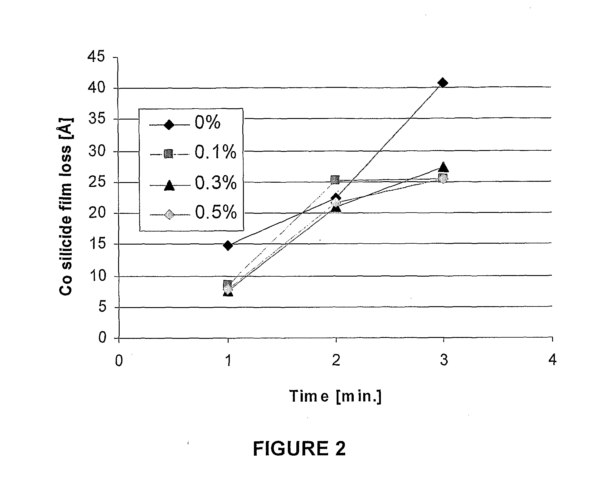
[0071]Subsequent to determining that anhydrous compositions were superior to hydrous compositions in terms of the selectivity of silicon oxide relative to both poly-Si and silicon nitride, the etch rate of silicon oxide, poly-Si and silicon nitride was determined using anhydrous compositions having varying base fluoride:acid fluoride component ratios.

[0072]The samples tested included 1 cm2 blanketed silicon oxide, poly-Si and silicon nitride, which were first measured using an optical interferometer (Nanospec) to determine the pre-immersion thickness, followed by individually immersing each wafer in approximately 50 mL of clean anhydrous composition, rinsing with deionized water, blowing dry with nitrogen and post-immersion measuring using the optical interferometer to determine the change in thickness to derive the etch rate of silicon oxide, poly-Si and silicon nitride in each composition. Silicon oxide was etched for 10 minutes whereas poly-Si and silicon nitride were etched for ...

example 2

[0076]Based on the results from Example 1, the base fluoride:acid fluoride ratio was further decreased and the ratio of TPGME to EG was varied. The experiments outlined in Example 1 were repeated for blanketed silicon oxide and poly-Si at 30° C. Silicon oxide was etched for 10 minutes whereas poly-Si was etched for 30 minutes.

[0077]The anhydrous compositions tested included B1-B4, as listed hereinbelow in Table 3.

TABLE 3Anhydrous compositions B1-B4.NH4HF2 / NH4F / TPGME / IDA / Solutionwt. %wt. %NH4F:HFwt. %wt. %EG / wt. %B12.52.53:10095B22.52.53:12192B32.52.53:16188B42.52.53:110184

[0078]The etch rates and the selectivity of anhydrous compositions B1-B4 at 30° C. are tabulated in Table 4 hereinbelow.

TABLE 4Etch rates of silicon oxide and poly-Si using compositions B1-B4.silicon oxidePoly-Si etchselectivityetch rate / rate / siliconSolutionÅ min−1Å min−1oxide:poly-SiB1259.53.6571:1B2274.63.4181:1B3270.43.090:1B4279.32.71103:1 

[0079]It can be seen that the higher the amount of glycol ether (TPGME) ...

example 3

[0080]Based on the results from Examples 1 and 2, various glycol ethers and other chelators were tested at various concentrations to determine the optimum chelator to add to said anhydrous composition. The experiments outlined in Example 1 were repeated for blanketed silicon oxide, poly-Si and silicon nitride at 30° C. Silicon oxide was etched for 10 minutes whereas poly-Si and silicon nitride were etched for 30 minutes.

[0081]The anhydrous compositions tested (C1-C12), each of which included 5 wt. % 3:1 NH4F:HF and 1 wt. % IDA, are listed hereinbelow in Table 5.

TABLE 5Anhydrous compositions C1-C12.TPGME / DPGPE / 400 MWtbutylEG / Solutionwt. %wt. %PEG / wt. %carbitol / wt. %wt. %C12000074C2000292C3000688C40001084C50002074C6020092C7060088C80100084C90200074C10001093C11002092C12004090

[0082]The etch rates and the selectivity of anhydrous compositions C1-C12 at 30° C. are tabulated in Table 6 hereinbelow.

TABLE 6Etch rates of silicon oxide, poly-Si and Si3N4 using compositions C1-C12.Poly-Siselecti...


PUM

PropertyMeasurementUnit
temperatureaaaaaaaaaa
pHaaaaaaaaaa

Abstract

A gate spacer oxide material removal composition and process for at least partial removal of gate spacer oxide material from a microelectronic device having same thereon. The anhydrous removal composition includes at least one organic solvent, at least one chelating agent, a base fluoride:acid fluoride component, and optionally at least one passivator. The composition achieves the selective removal of gate spacer oxide material relative to polysilicon and silicon nitride from the vicinity of the gate electrode on the surface of the microelectronic device with minimal etching of metal silicide interconnect material species employed in the gate electrode architecture.

Description

FIELD OF THE INVENTION[0001]The present invention relates to an anhydrous composition and method for at least partial removal of gate spacer oxide material from microelectronic devices, wherein the anhydrous compositions have a high selectivity for the gate spacer oxide material relative to both poly-silicon, silicon nitride and silicided interconnect materials.DESCRIPTION OF THE RELATED ART[0002]With the continued demand for improved device performance there is a continued emphasis on decreasing device dimensions, which provides the dual advantages of dramatically increasing device density as well as improving device performance. Device performance is improved because decreased device dimensions results in shorter paths that need to be traveled by charge carriers, e.g., electrons.[0003]For example, Metal-Oxide-Semiconductor Field-Effect Transistors (MOSFET) gate electrodes have as electrical points of contact the gate surface and the source and drain regions. The distance between t...

Claims


Application Information

Patent Timeline
Patent Type & Authority Applications(United States)
IPC IPC(8): C09K13/00
CPCH01L21/28052H01L21/31111H01L29/7833H01L29/6656H01L29/6659H01L29/6653C09K13/08
Inventor RAJARATNAM, MARTHA M.BERNHARD, DAVID D.MINSEK, DAVID W.
Owner ADVANCED TECH MATERIALS INC
Why Eureka
Try Eureka