Method and apparatus for tunable isotropic recess etching of silicon materials

a technology of isotropic recesses and silicon materials, which is applied in the electrical apparatus, semiconductor devices, basic electric elements, etc., can solve the problems of difficult control of positive slopes, less reproducibility, and difficult etching process used to remove a portion of silicon substrate, and achieve the effect of large top taper radius

Inactive Publication Date: 2009-02-05
APPLIED MATERIALS INC
View PDF12 Cites 61 Cited by
  • Summary
  • Abstract
  • Description
  • Claims
  • Application Information

AI Technical Summary

Benefits of technology

[0010]Recess etch methods and apparatuses are described herein. In particular embodiments, these methods may be employed to form recesses in a silicon substrate having an isotropic character to undercut a transistor in preparation for a source/drain regrowth. In one embodiment, an at least partially isotropic plasma recess etch is performed to provide a recess adjacent to the channel region of the transistor. In certain embodiments, the recess has a V/L ratio of between 1.1 and 2.2. In a particular embodiment, as shown in FIG. 4E, the plasma condition provides a recess having a sufficiently large top taper radius that the recess sidewall is not re-

Problems solved by technology

Many constraints make the etch process used to remove a portion of the silicon substrate, referred to herein as the “recess etch,” particularly challenging.
Such positive slopes can be difficult to control and less reproducible across a substrate and between substrates.
Furthermore, the maximum depth of the recess, Drecess, is limited by the implanted well 117 having a depth only a few times the maximum distance to be laterally undercut by the recess etch, Dundercut.
Further constraints on the recess etch process include integration issues, such as, a general incompatibility between shallow trench isolation and epitaxial source/drain regrowth where the recess interfaces with the isolation 120, shown in FIG

Method used


Image

  • Method and apparatus for tunable isotropic recess etching of silicon materials
  • Method and apparatus for tunable isotropic recess etching of silicon materials
  • Method and apparatus for tunable isotropic recess etching of silicon materials

Examples


Embodiment Construction

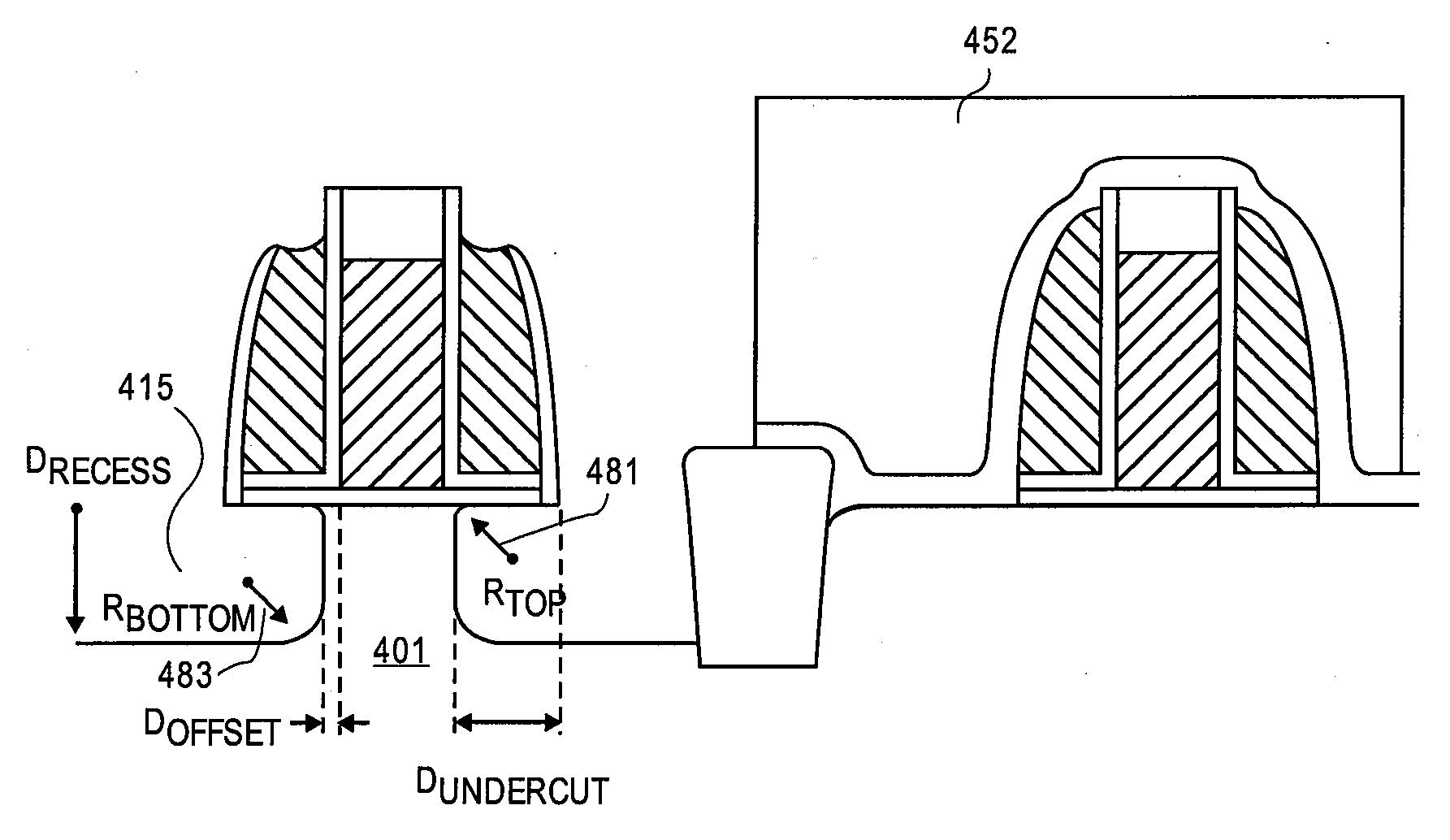
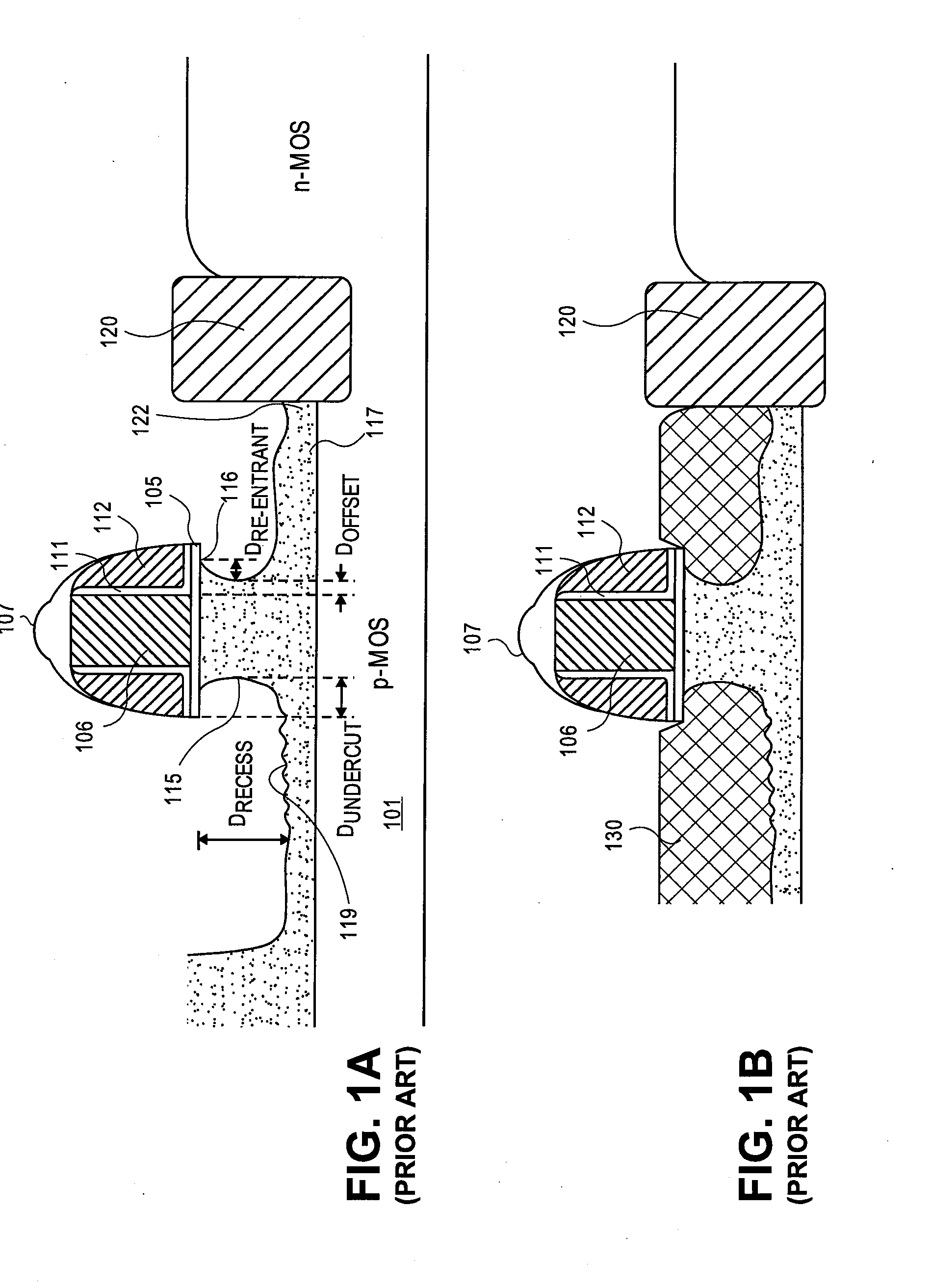
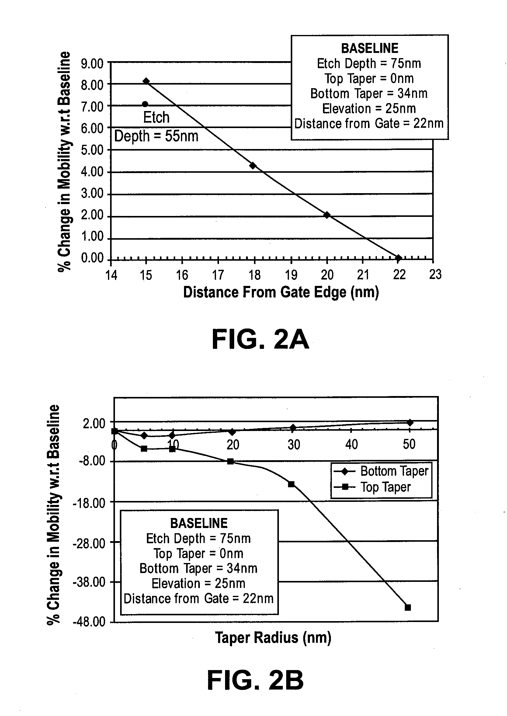
[0020]Embodiments of recess etch methods are described herein with reference to figures. However, particular embodiments may be practiced without one or more of these specific details, or in combination with other known methods, materials, and apparatuses. In the following description, numerous specific details are set forth, such as specific materials, dimensions and processes parameters etc. to provide a thorough understanding. In other instances, well-known semiconductor processes and manufacturing techniques have not been described in particular detail to avoid unnecessarily obscuring the claimed subject matter. Reference throughout this specification to “an embodiment” means that a particular feature, structure, material, or characteristic described in connection with the embodiment is included in at least one embodiment of the invention. Thus, the appearances of the phrase “in an embodiment” in various places throughout this specification are not necessarily referring to the s...


PUM


Abstract

Methods and apparatuses to etch recesses in a silicon substrate having an isotropic character to undercut a transistor in preparation for a source/drain regrowth. In one embodiment, a cap layer of a first thickness is deposited over a transistor gate stack and spacer structure. The cap layer is then selectively etched in a first region of the substrate, such as a p-MOS region, using a first isotropic plasma etch process and a second anisotropic plasma etch process. In another embodiment, an at least partially isotropic plasma recess etch is performed to provide a recess adjacent to the channel region of the transistor. In a particular embodiment, the plasma etch process provides a recess sidewall that is neither positively sloped nor more than 10 nm re-entrant.

Description

BACKGROUND[0001]1. Field[0002]Embodiments described herein relate to the electronics manufacturing industry and more particularly to the etching of recesses in a substrate, such as one used in integrated circuit (IC) fabrication.[0003]2. Discussion of Related Art[0004]Locally strained silicon on p-MOS transistors has been found to improve carrier mobility up to 50% in 90 nm logic devices. Locally strained silicon generally entails removing a portion of the silicon substrate 101 about the gate stack of a p-MOS transistor, the gate stack having a gate dielectric 105, a gate electrode 106 and a gate hardmask 107. As shown in FIG. 1A, the recess 115 thereby undercuts the spacer 112. Subsequently, an epitaxial silicon-germanium allows (SiGe) source / drain 130 is grown in the recess 115, as shown in FIG. 1B. The SiGe induces a compressive uniaxial strain on the silicon under the gate stack which enhances hole mobility in the silicon channel of the p-MOS device.[0005]Many constraints make t...

Claims


Application Information

Patent Timeline
IPC IPC(8): H01L29/94H01L21/302H01L21/311
CPCH01L21/3065H01L21/823807H01L29/7848H01L29/6656H01L29/66636H01L21/823814
Inventor KAWAGUCHI, MARK NAOSHISHEN, MEIHUASASANO, HIROKICHEN, RONG
Owner APPLIED MATERIALS INC
Why Eureka
Try Eureka