White organic light emitting device

Active Publication Date: 2009-02-05
SAMSUNG DISPLAY CO LTD
View PDF12 Cites 58 Cited by
  • Summary
  • Abstract
  • Description
  • Claims
  • Application Information

AI Technical Summary

Benefits of technology

[0020]The present invention provides a white organic light emitting device emitting light that has no c

Problems solved by technology

However, energy transfer into dopants generally is inefficient, and therefore is incomplete.
However, adjusting the color balance that results in white emission can not be easily adjusted.
However, white is obtained using the complementary colors, and thus realizing full colors using color filters is difficult and the range of colors that can be expressed is narrow.
Whereas, in the case of the 3-wavelength white organic light emitting device, due to energy transfer between molecules, a uniform spectrum of three colors, that is, red, green and blue, can not generally be achieved and therefore light emission efficiency remains low.
The white organic light emitting device is manufactured using a simple manufacturing process, but it st

Method used


Image

  • White organic light emitting device
  • White organic light emitting device
  • White organic light emitting device

Examples


example 1

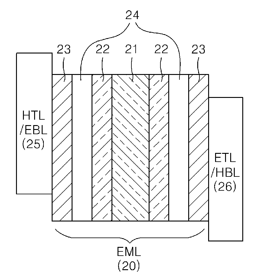
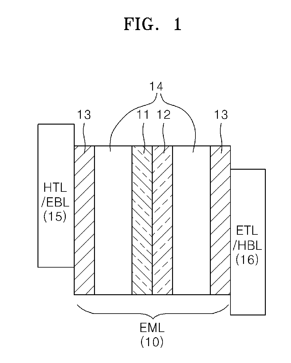
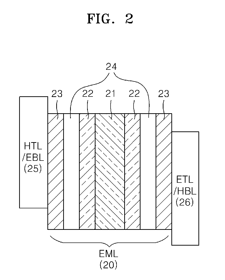
[0082]A 15 Ω / cm2 (1,000 Å) ITO-glass substrate used as an anode was cut to a size of 50 mm×50 mm×0.7 mm. The prepared substrate was ultrasonically cleaned in acetone, isopropyl alcohol and pure water, for 15 minutes each, and then further cleaned by exposure to ultraviolet (UV) rays for 30 minutes. NPB was vacuum deposited on the substrate to form a hole transport layer having a thickness of 400 Å. An emissive layer was formed on the hole transport layer by using the following processes: CBP as a host and BCzVBi as a dopant were vacuum deposited together on the hole transport layer in a weight ratio of 5 to 1 , respectively, to form a blue emissive layer having a thickness of 100 Å; 40 Å of CBP as a host was vacuum deposited thereon to form a spacer layer; CBP as a host and 5 wt % Ir(ppy)3 as a dopant were vacuum deposited together thereon, respectively, to form a green emissive layer having a thickness of 30 Å; 2 Å of CBP as a host was vacuum deposited thereon to form a spacer laye...

example 2

[0083]A white organic light emitting device was manufactured in the same manner as in Example 1, except that a spacer layer was not formed between a green emissive layer and a red emissive layer.


PUM

PropertyMeasurementUnit
Thicknessaaaaaaaaaa
Thicknessaaaaaaaaaa
Thicknessaaaaaaaaaa

Abstract

Provided is a white organic light emitting device including an anode, a cathode and an organic layer disposed therebetween, the organic layer having a structure wherein an arrangement of a green emissive layer and a blue emissive layer is formed on both surfaces of a red emissive layer such that the resultant structure is symmetrical around the red emissive layer, and a spacer layer is disposed between opposing surfaces of the blue emissive layer and the green emissive layer, where the white organic light emitting device including this structure exhibits a constant luminescence spectra irrespective of any change in current density. A method of forming the white organic light emitting device is also disclosed.

Description

[0001]This application claims priority to Korean Patent Application No. 10-2007-0006303, filed on Jan. 19, 2007, and all the benefits accruing therefrom under 35 U.S.C. § 119, the content of which is incorporated herein by reference in its entirety.BACKGROUND OF THE INVENTION[0002]1. Field of the Invention[0003]The present invention relates to a white organic light emitting device, and more particularly, to a white organic light emitting device emitting light having a color which is not affected by a change in current, has excellent luminescence efficiency, and long lifespan.[0004]2. Description of the Related Art[0005]Organic light emitting devices are self-emissive devices which use electroluminescence, and have high recognition ability, and are complete solid devices having excellent impact resistance. Therefore, organic light emitting devices have gained a great deal of attention and have been used in a variety of different kinds of display devices.[0006]Organic light emitting d...

Claims


Application Information

Patent Timeline
IPC IPC(8): H01J1/63
CPCH01L51/001H01L51/0072H01L51/0085Y10S428/917H01L51/5016H01L51/5036H01L2251/308H01L51/50H10K71/164H10K85/342H10K85/6572H10K50/00H10K50/125H10K50/11H10K2101/10H10K2102/103A41B11/121A41B11/123A41B11/001A41B2400/82
Inventor AHN, PIL-SOOKIM, SANG-YEOL
Owner SAMSUNG DISPLAY CO LTD
Why Eureka
Try Eureka