Methods of for forming ultra thin structures on a substrate

a technology of ultra thin structures and substrates, applied in the direction of basic electric elements, semiconductor/solid-state device manufacturing, electric devices, etc., can solve the problems of anisotropic striation formation, difficult critical dimension and etch profile control, and significant research investment and integration costs of new lithographic tools and techniques, so as to reduce the critical dimension of an opening and reduce the dimension

Inactive Publication Date: 2009-02-05
APPLIED MATERIALS INC
View PDF8 Cites 45 Cited by
  • Summary
  • Abstract
  • Description
  • Claims
  • Application Information

AI Technical Summary

Benefits of technology

[0011]In one embodiment, a method of forming a submicron structure on a substrate may include providing a substrate having a patterned photoresist layer disposed on a film stack into an etch chamber, wherein the film stack includes at least a hardmask layer disposed on a dielectric layer, performing a polymer deposition process to deposit a polymer layer on the pattered photoresist layer, thus reducing a critical dimension of an opening in the patterned photoresist layer, and etching the underlying hardmask layer through the opening having the reduced dimension.

Problems solved by technology

Reliably producing sub-half micron and smaller features is one of the key technology challenges for next generation very large scale integration (VLSI) and ultra large-scale integration (ULSI) of semiconductor devices.
However, as the limits of circuit technology are pushed, the shrinking dimensions of VLSI and ULSI interconnect technology have placed additional demands on processing capabilities.
Developing new lithographic tools and techniques pose significantly research investment and integration cost.
However, with shrinking geometries, precise critical dimension and etch profile control have become increasingly difficult.
One problem found during plasma submicron 55 nm etching processes is control of the sidewall roughness of the etched structure, which may result in formation of anisotropic striation.
As the dimensions of the features continue to diminish, sidewall striation and / or post-etch sidewall roughness occurrence in small critical dimension structures pose a significant challenge to structure profile integrity, which may ultimately deteriorate overall device performance.

Method used


Image

  • Methods of for forming ultra thin structures on a substrate
  • Methods of for forming ultra thin structures on a substrate
  • Methods of for forming ultra thin structures on a substrate

Examples


Embodiment Construction

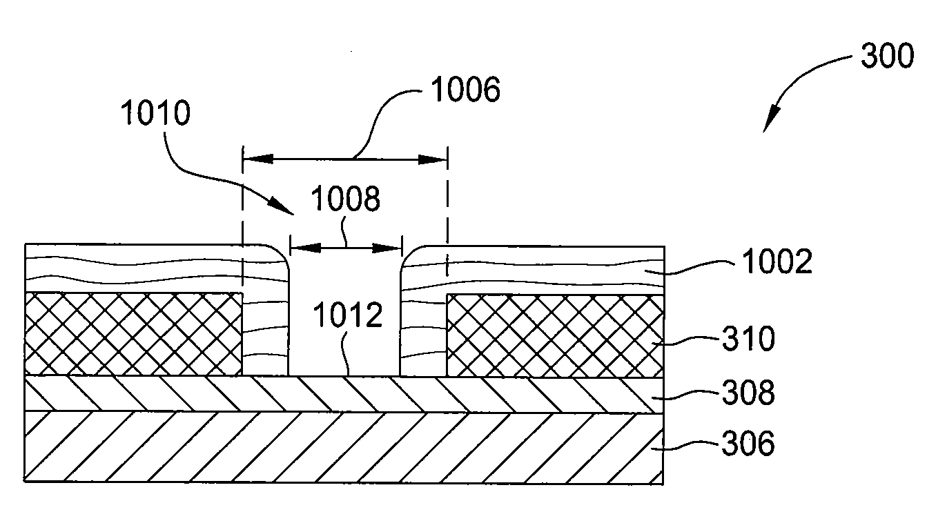
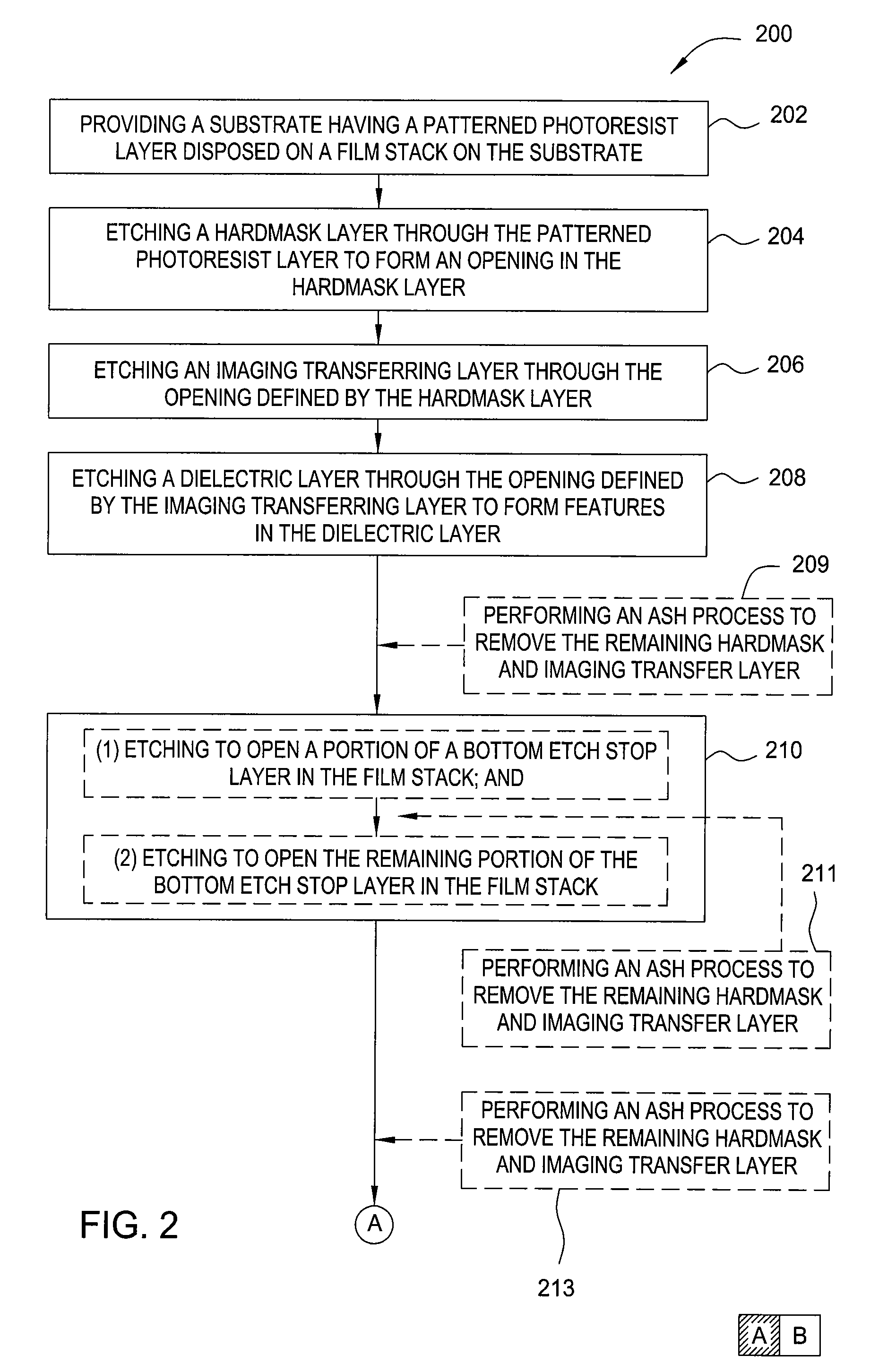
[0026]Embodiments of the invention generally relate to methods for forming an ultra thin structure on a substrate substantially without sidewall striation and critical dimension loss. In one embodiment, the ultra thin structure formed using at least one cycle of polymer deposition of photoresist (PDP) and etching to form structures with a critical dimension down to 55 nm or less within a dielectric layer. In some embodiments, multiple cycles of polymer deposition of photoresist (PDP) and etching may be used. The method described herein includes a sequential polymer deposition of photoresist (PDP) process and followed by an etching process to gradually etch the underlying layers while maintaining control of features geometry as well as high feature aspect ratio. The method also maintains control of critical dimension transfer as well as retaining good sidewall profile control.

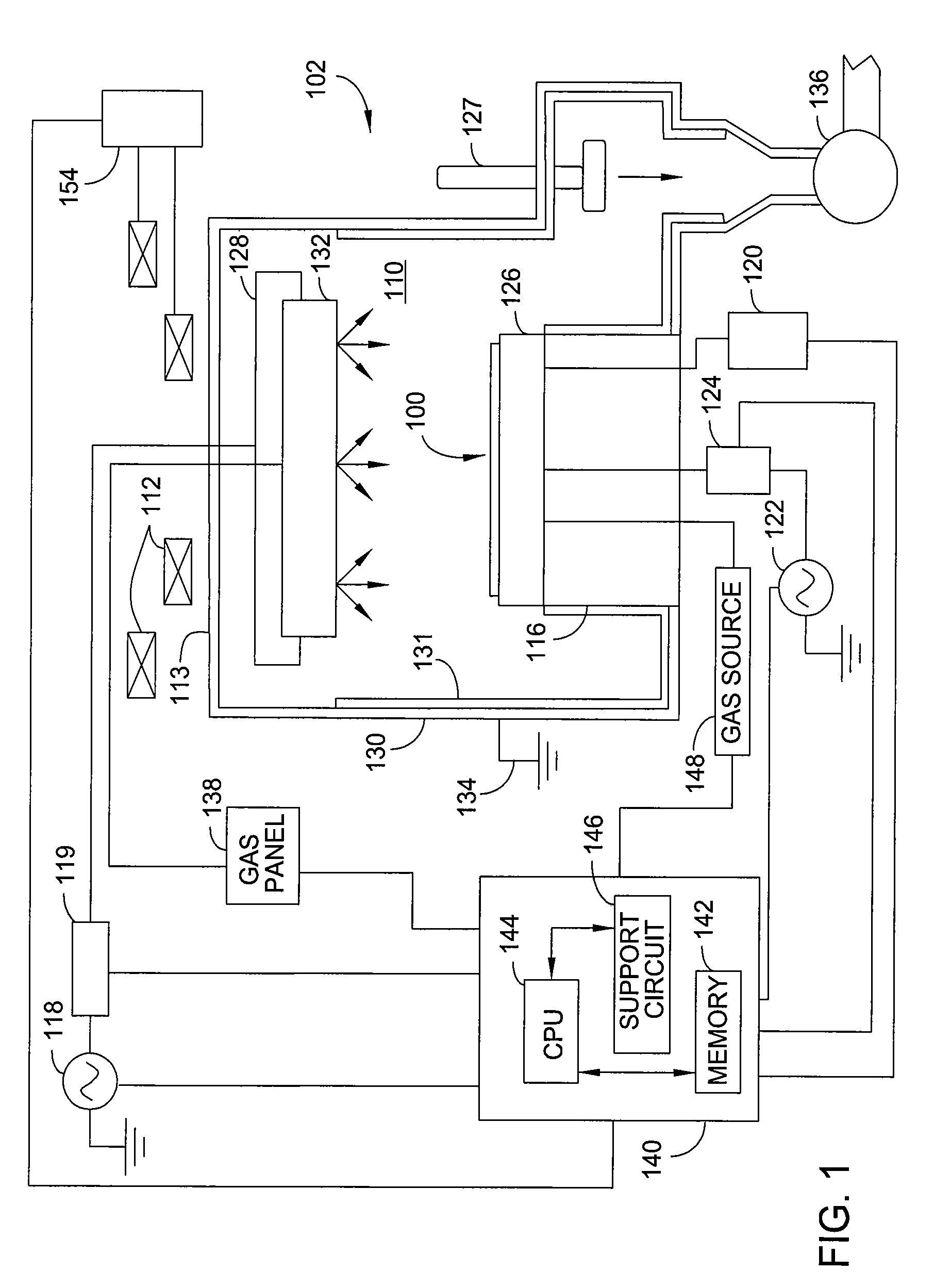
[0027]The etch and deposition process described herein may be performed in any suitably adapted plasma etch c...


PUM

PropertyMeasurementUnit
roughnessaaaaaaaaaa
frequencyaaaaaaaaaa
frequencyaaaaaaaaaa

Abstract

Methods for forming an ultra thin structure using a method that includes multiple cycles of polymer deposition of photoresist (PDP) process and etching process. The embodiments described herein may be advantageously utilized to fabricate a submicron structure on a substrate having a critical dimension less than 55 nm and beyond. In one embodiment, a method of forming a submicron structure on a substrate may include providing a substrate having a patterned photoresist layer disposed on a film stack into an etch chamber, wherein the film stack includes at least a hardmask layer disposed on a dielectric layer, performing a polymer deposition process to deposit a polymer layer on the pattered photoresist layer, thus reducing a critical dimension of an opening in the patterned photoresist layer, and etching the underlying hardmask layer through the opening having the reduced dimension.

Description

CROSS-REFERENCE TO RELATED APPLICATIONS[0001]This application claims benefit of U.S. Provisional Application Ser. No. 60 / 948,471, filed Jul. 8, 2007 (Attorney Docket No. APPM / 12236L) and U.S. Provisional Application Ser. No. 60 / 949,835, filed Jul. 13, 2007 (Attorney Docket No. APPM / 12236L02), both of which are incorporated by reference in their entirety.BACKGROUND[0002]1. Field[0003]Embodiments of the present invention generally relates to methods for forming ultra thin structures on a substrate, and more specifically, for using multiple cycles of polymer deposition of photoresist (PDP) and etching to form ultra thin structures on a substrate suitable for semiconductor device fabrication.[0004]2. Description of the Related Art[0005]Reliably producing sub-half micron and smaller features is one of the key technology challenges for next generation very large scale integration (VLSI) and ultra large-scale integration (ULSI) of semiconductor devices. However, as the limits of circuit te...

Claims


Application Information

Patent Timeline
Patent Type & Authority Applications(United States)
IPC IPC(8): H01L21/311
CPCH01L21/02063H01L21/0337H01L21/76802H01L21/31116H01L21/31144H01L21/0338
Inventor CHIANG, KANG-LIEKAO, CHIA-LING
Owner APPLIED MATERIALS INC
Why Eureka
Try Eureka