Semiconductor device property extraction, generation, visualization, and monitoring methods

a technology of semiconductor devices and properties, applied in the direction of material analysis, measurement arrangements of variables, instruments, etc., can solve the problems of inability to inspect patterned wafers, failure and inability to detect defects of decreasing siz

Active Publication Date: 2009-02-05
KLA TENCOR TECH CORP
View PDF40 Cites 133 Cited by
  • Summary
  • Abstract
  • Description
  • Claims
  • Application Information

AI Technical Summary

Benefits of technology

[0032]In one embodiment, the image of the surface of the patterned wafer includes an image of substantially an entire surface of the patterned wafer. In another embodiment, the image of the surface of the patterned wafer is substantially free of pattern misregistration noise. In an additional embodiment, the image of the surface of the patterned wafer includes a gray scale image of intensity of light scattered from the patterned wafer. In a further embodiment, the image of the surface of the patterned wafer includes a noise map of the surface of the patterned wafer.

Problems solved by technology

However, as the dimensions of semiconductor devices decrease, inspection becomes even more important to the successful manufacture of acceptable semiconductor devices because smaller defects can cause the device to fail.
For instance, as the dimensions of semiconductor devices decrease, detection of defects of decreasing size has become necessary since even relatively small defects may cause unwanted aberrations in the semiconductor devices.
Since these tools are optimized for inspecting unpatterned wafers, these tools are generally not capable of inspecting patterned wafers for a number of reasons.
As such, the single detector may become saturated and, consequently, will not yield signals that can be analyzed for defect detection.
In addition, even if the single detector does not become saturated, the light scattered from patterns or other features on the wafer cannot be separated from other scattered light thereby hindering, if not preventing, defect detection based on the other scattered light.
Although inspection of unpatterned wafers, or “monitor wafers,” which have been run through a process tool, may be used as a gauge for the number and types of defects that may be found on patterned wafers, or “product wafers,” defects detected on monitor wafers do not always accurately reflect the defects that are detected on patterned wafers after the same process in the process tool.
There are, however, a number of disadvantages to using metrology processes and tools to measure one or more characteristics of a wafer for process monitoring and control applications.
For example, most metrology tools are relatively slow, particularly compared to inspection systems.
As such, using metrology measurements performed at one location or a limited number of locations on a wafer may not provide sufficient information about the characteristic(s) of the wafers such that the process can be accurately monitored and controlled.
Furthermore, using metrology tools to measure characteristics across the wafer for inline monitoring and control applications is not feasible due to the time in which such measurements can be performed.
In particular, metrology measurements performed by currently available metrology tools such as surface roughness, resistivity, film thickness, etc. are not suitable for high sampling of wafers for inline monitoring since the measurements will impact (e.g., increase) cycle time in production.

Method used


Image

  • Semiconductor device property extraction, generation, visualization, and monitoring methods
  • Semiconductor device property extraction, generation, visualization, and monitoring methods
  • Semiconductor device property extraction, generation, visualization, and monitoring methods

Examples


Embodiment Construction

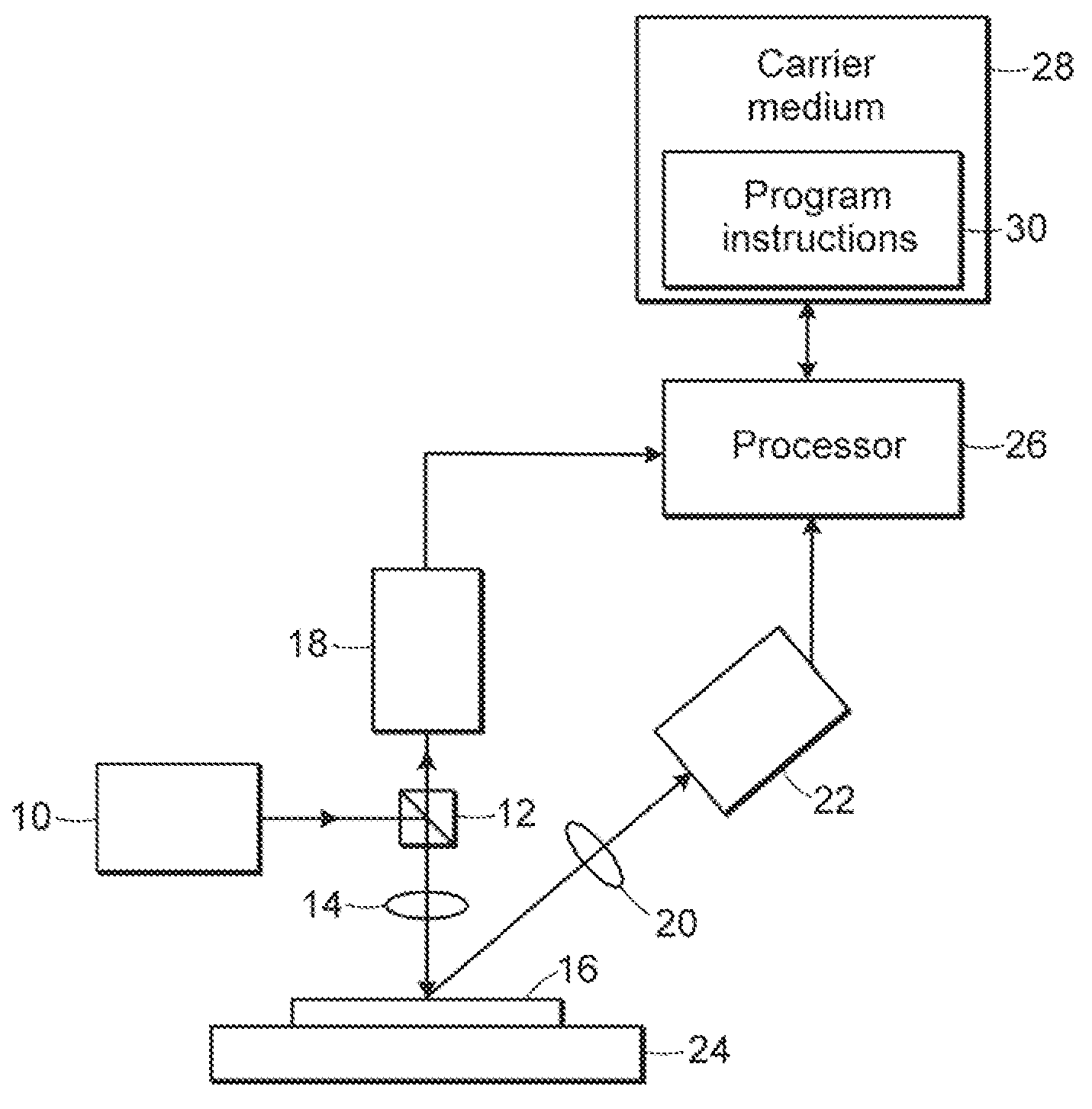
[0064]As used herein, the term “specimen” generally refers to a wafer, a photomask, or a reticle. However, it is to be understood that the methods, carrier media, and systems described herein may be used for monitoring a characteristic of any other specimen known in the art.

[0065]As used herein, the term “wafer” generally refers to substrates formed of a semiconductor or non-semiconductor material. Examples of such a semiconductor or non-semiconductor material include, but are not limited to, monocrystalline silicon, gallium arsenide, and indium phosphide. Such substrates may be commonly found and / or processed in semiconductor fabrication facilities.

[0066]A wafer may include one or more layers formed upon a substrate. For example, such layers may include, but are not limited to, a resist, a dielectric material, a conductive material, and a semiconductor material. Many different types of such layers are known in the art, and the term wafer as used herein is intended to encompass a wa...


PUM


Abstract

Various methods, carrier media, and systems for monitoring a characteristic of a specimen are provided. One computer-implemented method for monitoring a characteristic of a specimen includes determining a property of individual pixels on the specimen using output generated by inspecting the specimen with an inspection system. The method also includes determining a characteristic of individual regions on the specimen using the properties of the individual pixels in the individual regions. The method further includes monitoring the characteristic of the specimen based on the characteristics of the individual regions.

Description

BACKGROUND OF THE INVENTION[0001]1. Field of the Invention[0002]The present invention generally relates to methods, carrier media, and systems for monitoring a characteristic of a specimen. Certain embodiments relate to determining a characteristic of individual regions on a specimen using properties of individual pixels in the individual regions and monitoring a characteristic of the specimen based on the characteristics of the individual regions.[0003]2. Description of the Related Art[0004]The following description and examples are not admitted to be prior art by virtue of their inclusion in this section.[0005]Fabricating semiconductor devices such as logic and memory devices typically includes processing a specimen such as a semiconductor wafer using a number of semiconductor fabrication processes to form various features and multiple levels of the semiconductor devices. For example, lithography is a semiconductor fabrication process that typically involves transferring a pattern...

Claims


Application Information

Patent Timeline
Patent Type & Authority Applications(United States)
IPC IPC(8): G06F15/00
CPCG01N21/9501
Inventor KULKARNI, ASHOKCAMPOCHIARO, CECELIAWALLINGFORD, RICHARDZHANG, YONGDUFFY, BRIAN
Owner KLA TENCOR TECH CORP
Why Eureka
Try Eureka