Semiconductor device

a semiconductor and device technology, applied in semiconductor devices, digital storage, instruments, etc., can solve the problems of unstable rewriting characteristics, inability to meet the requirements of the device, and the concentration of ag, cu, or the like in the solid electrolyte becomes too high, so as to improve the performance of the semiconductor device

Inactive Publication Date: 2009-02-12
HITACHI LTD
View PDF6 Cites 39 Cited by
  • Summary
  • Abstract
  • Description
  • Claims
  • Application Information

AI Technical Summary

Benefits of technology

[0006]An object of the present invention is to provide a technique capable of improving the performance of a semiconductor device capable of storing information.
[0011]Performance of a semiconductor device capable of storing information can be improved.

Problems solved by technology

However, when rewriting of the memory is repeated, metal ions diffuse from the metal electrodes into the solid electrolyte so that the shape of the electrode surfaces is changed in the atomic level, and thus rewriting characteristics become unstable and the resistance may be varied every time of rewrite.
In addition, when rewrite of the memory is repeated, the concentration of Ag, Cu, or the like in the solid electrolyte becomes too high due to the diffusion from the electrodes, and there is a possibility that the resistance is not changed from a middle intermediate resistance between ON and OFF.
These problems deteriorate the performance of the semiconductor device which can store information.

Method used


Image

  • Semiconductor device
  • Semiconductor device
  • Semiconductor device

Examples


first embodiment

[0069]A semiconductor device of an embodiment of the present invention and a fabrication method thereof will be described with reference to the accompanied drawings.

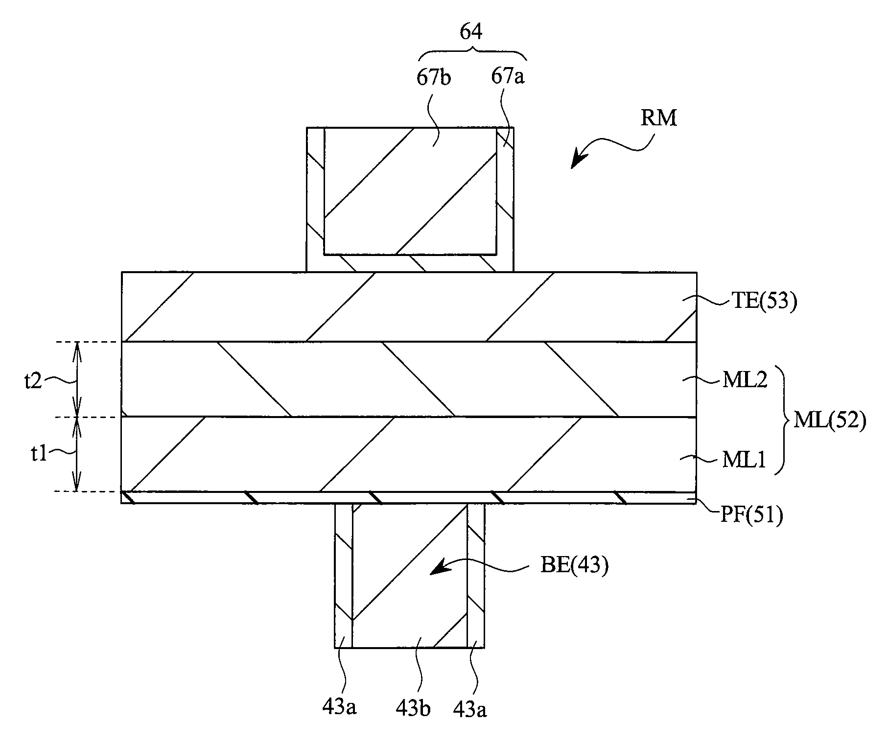
[0070]FIG. 1 is an explanatory diagram (cross sectional view) schematically showing a memory element in the semiconductor device of the present embodiment. In FIG. 1, to facilitate understanding, illustration of insulating films (corresponding to insulating films 41, 61, and 62, which will be described later) surrounding the periphery of the memory element RM is omitted.

[0071]As shown in FIG. 1, the memory element (storage element) RM of the present embodiment has a memory layer (recording layer, memory material layer) ML, a bottom electrode (plug-type electrode, conductive portion, first electrode) BE, and a top electrode (top electrode film, conductive portion, second electrode) TE, and the bottom and top electrodes are respectively formed on both surfaces (mutually opposite surfaces, which are the lower surface and th...

second embodiment

[0239]FIG. 32 is an explanatory diagram (cross sectional view) schematically showing a memory element RM in a semiconductor device according to the present embodiment and corresponds to FIG. 1 of the above-described first embodiment. FIG. 33 is an explanatory diagram (graph, triangular diagram, composition diagram) showing a desired composition range of the material forming a top electrode TE1 in the memory element RM of the present embodiment.

[0240]The memory element RM of the present embodiment shown in FIG. 32 has an approximately same constitution as the memory element RM of the above-described first embodiment except that the top electrode TE1 having a material different from that of the top electrode TE is used instead of the top electrode TE; therefore, the explanations thereof will be omitted herein except for some descriptions about the material of the top electrode TE1.

[0241]In the memory element RM of the present embodiment, the top electrode TE1 also has a function as an...

third embodiment

[0267]FIG. 38 is an explanatory diagram (cross sectional view) schematically showing a memory element RM in a semiconductor device according to the present embodiment and corresponds to FIG. 1 of the above-described first embodiment.

[0268]The memory element RM of the present embodiment shown in FIG. 38 has an approximately same constitution as the memory element RM of the first embodiment except that the first layer ML1 of the memory layer ML has a stacked structure of a plurality of layers having mutually different compositions. Therefore, except for a description about the first layer ML1 of the memory layer ML, descriptions thereof will be omitted.

[0269]In the first embodiment, the first layer ML1 of the memory layer ML has a single-layer structure. However, in the present embodiment, as shown in FIG. 38, the first layer ML1 of the memory layer ML is formed by a plurality of layers (chalcogenide layers) having mutually different compositions. In FIG. 38 and in the description bel...


PUM


Abstract

The performance of a semiconductor device capable of storing information is improved. A memory layer of a memory element is formed by a first layer at a bottom electrode side and a second layer at a top electrode side. The first layer contains 20-70 atom % of at least one element of a first element group of Cu, Ag, Au, Al, Zn, and Cd, contains 3-40 atom % of at least one element of a second element group of V, Nb, Ta, Cr, Mo, W, Ti, Zr, Hf, Fe, Co, Ni, Pt, Pd, Rh, Ir, Ru, Os, and lanthanoid elements, and contains 20-60 atom % of at least one element of a third element group of S, Se, and Te. The second layer contains 5-50 atom % of at least one element of the first element group, 10-50 atom % of at least one element of the second element group, and 30-70 atom % of oxygen.

Description

CROSS-REFERENCE TO RELATED APPLICATION[0001]The present application claims priority from Japanese Patent Application No. JP 2007-206890 filed on Aug. 8, 2007, the content of which is hereby incorporated by reference into this application.TECHNICAL FIELD OF THE INVENTION[0002]The present invention relates to a semiconductor device. More particularly, the present invention relates to a semiconductor device having a non-volatile storage element.BACKGROUND OF THE INVENTION[0003]A non-volatile memory called a polarized memory or a solid electrolyte memory has been known (for example, see Japanese Patent Application Laid-Open Publication No. 2005-197634 (Patent Document 1); T. Sakamoto, S. Kaeriyama, H. Sunamura, M. Mizuno, H. Kawaura, T. Hasegawa, K. Terabe, T. Nakayama and M. Aono, “2004 IEEE International Solid State Circuits Conference (ISSCC)”, Digest of Technical Papers, USA, 2004, No. 16.3, p. 290 (Non-Patent Document 1); and M. N. Kozicki, C. Gopalan, M. Balakrishnan, M. Park, and...

Claims


Application Information

Patent Timeline
Patent Type & Authority Applications(United States)
IPC IPC(8): H01L45/00
CPCG11C11/5614H01L45/1675G11C13/0069G11C2013/0083G11C2213/11G11C2213/15G11C2213/56G11C2213/79H01L27/24H01L27/2436H01L27/2463H01L45/085H01L45/141H01L45/142H01L45/143H01L45/144G11C13/0011H10B63/30H10B63/80H10N70/245H10N70/8416H10N70/8822H10N70/882H10N70/063H10N70/826G11C13/0004H10N70/8825H10N70/8828
Inventor TERAO, MOTOYASUSASAGO, YOSHITAKAKUROTSUCHI, KENZOONO, KAZUOFUJISAKI, YOSHIHISATAKAURA, NORIKATSUTAKEMURA, RIICHIRO
Owner HITACHI LTD
Why Eureka
Try Eureka