Non-volatile memory and manufacturing method thereof

a non-volatile memory and manufacturing method technology, applied in the field of memory, can solve the problems of reducing the dimension of the memory, the coupling ratio between a control gate and a floating gate in the non-volatile memory drops significantly, and the coupling ratio cannot be substantially improved to meet the increasingly advanced requirements, so as to increase the overlap area

Inactive Publication Date: 2009-02-19
NAN YA TECH
View PDF4 Cites 0 Cited by
  • Summary
  • Abstract
  • Description
  • Claims
  • Application Information

AI Technical Summary

Benefits of technology

[0010]In view of the foregoing shortcomings, the present invention is directed to a manufacturing method of a non-volatile memory to solve the problem incurred by the coupling ratio between the control gate and floating gates. The manufacturing method is able to increase an overlapping area between the control gate and the floating gate via an improved three-dimensional manufacturing process.

Problems solved by technology

However, as semiconductor devices are continuously miniaturized and line widths of the devices are reduced, dimensions of the memories are also decreased, such that a coupling ratio between a control gate and a floating gate in the non-volatile memory drops significantly.
Nevertheless, in the aforesaid non-volatile memory, even though the disposition of the control gate is utilized, the coupling ratio cannot be substantially improved to meet the increasingly advanced requirements.

Method used


Image

  • Non-volatile memory and manufacturing method thereof
  • Non-volatile memory and manufacturing method thereof
  • Non-volatile memory and manufacturing method thereof

Examples


Embodiment Construction

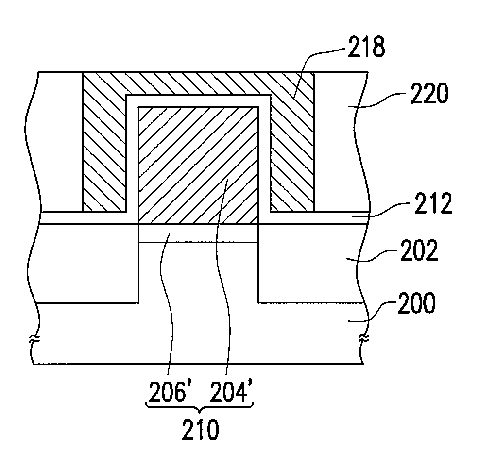
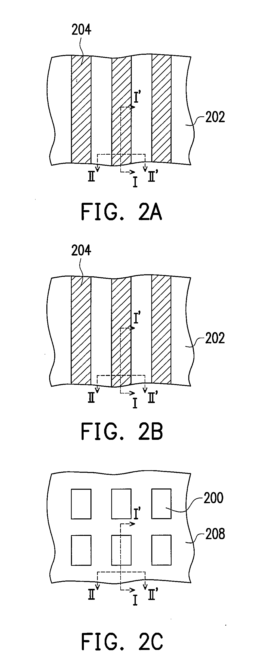
[0032]FIGS. 2A through 2F are top views illustrating a process of manufacturing a non-volatile memory according to an embodiment of the present invention. FIGS. 3A through 3F are cross-sectional views illustrating the process of manufacturing the non-volatile memory along a I-I′ cross-section in FIGS. 2A through 2F. FIGS. 4A through 4F are cross-sectional views illustrating the process of manufacturing the non-volatile memory along a II-II′ cross-section in FIGS. 2A through 2F.

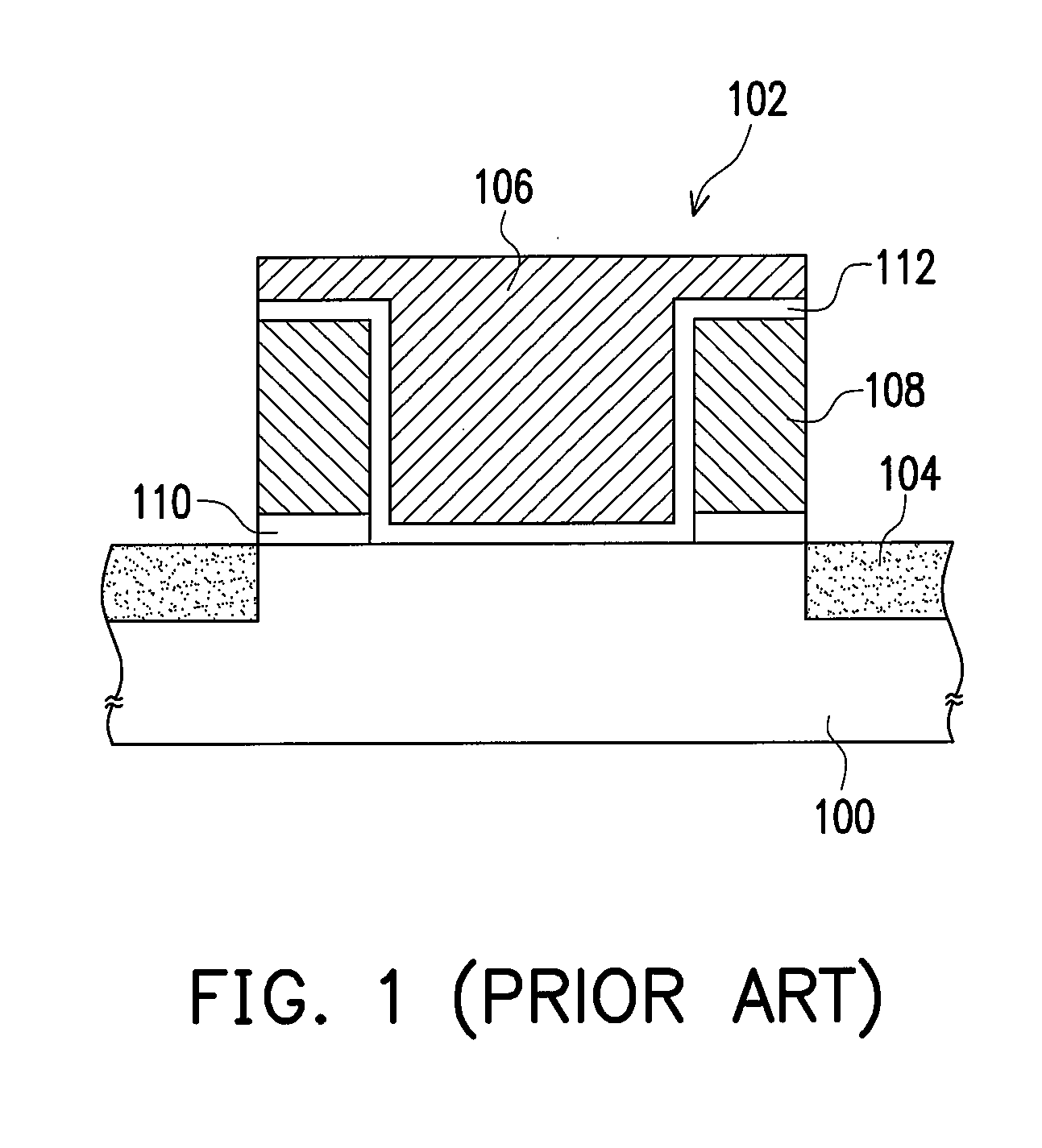
[0033]First, referring concurrently to FIGS. 2A, 3A and 4A, a substrate 200 is provided. The substrate 200 is, for example, a silicon substrate. Next, a dielectric layer (now shown) and a conductive layer (now shown) are sequentially formed on the substrate 200. A material of the dielectric layer is oxide, for example, and the dielectric layer is formed, for example, by thermal oxidation. A material of the conductive layer is, for example, polysilicon, and the conductive layer is formed by performing a chemica...


PUM


Abstract

A non-volatile memory having a gate structure and a source/drain region is provided. The gate structure is disposed on a substrate. The gate structure includes a pair of floating gates, tunneling dielectric layers, a control gate and an inter-gate dielectric layer. The floating gates are disposed on the substrate. Each tunneling dielectric layer is disposed between each floating gate and the substrate. The control gate is disposed on the substrate between the pair of the floating gates and covers a top surface and sidewalls of each floating gate. The inter-gate dielectric layer is disposed between the control gate and each of the floating gates, disposed between the control gate and each of the tunneling dielectric layers, and disposed between the control gate and the substrate. The source/drain region is disposed in the substrate at respective sides of the gate structure.

Description

CROSS-REFERENCE TO RELATED APPLICATION[0001]This application claims the priority benefit of Taiwan application serial no. 96129849, filed on Aug. 13, 2007. The entirety of the above-mentioned patent application is hereby incorporated by reference herein and made a part of this specification.BACKGROUND OF THE INVENTION[0002]1. Field of the Invention[0003]The present invention relates to a memory and a manufacturing method thereof. More particularly, the present invention relates to a non-volatile memory and a manufacturing method thereof.[0004]2. Description of Related Art[0005]A non-volatile memory allows multiple data writing, reading and erasing operations. The stored data in the non-volatile memory will still be retained even after power to a device using the non-volatile memory is off. With these advantages, the non-volatile memory has become one of the most widely adopted memories for personal computers and electronic equipment. However, as semiconductor devices are continuousl...

Claims


Application Information

Patent Timeline
Patent Type & Authority Applications(United States)
IPC IPC(8): H01L21/336
CPCH01L27/11521H10B41/30
Inventor LIAO, WEI-MINGCHANG, MING-CHENGHUANG, CHIEN-CHANG
Owner NAN YA TECH
Why Eureka
Try Eureka