Method and Structure for Shielded Gate Trench FET

a shielded gate trench and trench structure technology, applied in the field of shielded gate trench fet, can solve the problems of difficult to obtain the desired ied thickness, cvd process tends to produce lower quality dielectrics, higher charges and traps,

Active Publication Date: 2009-02-26
SEMICON COMPONENTS IND LLC
View PDF15 Cites 60 Cited by
  • Summary
  • Abstract
  • Description
  • Claims
  • Application Information

AI Technical Summary

Problems solved by technology

Each of these methods has limitations.
For example, the CVD process tends to produce lower quality dielectric and higher charges and traps.
As a result, even though thermal oxidation often produces higher quality oxide, it is difficult to obtain the desired IED thickness.

Method used


Image

  • Method and Structure for Shielded Gate Trench FET
  • Method and Structure for Shielded Gate Trench FET
  • Method and Structure for Shielded Gate Trench FET

Examples


Embodiment Construction

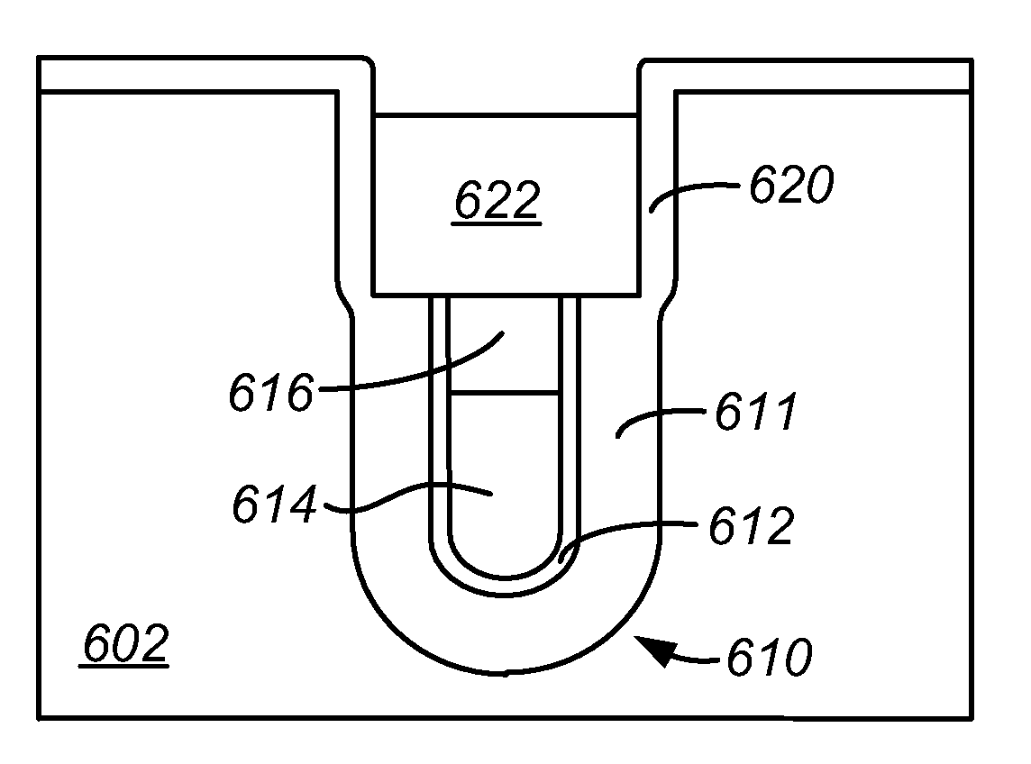
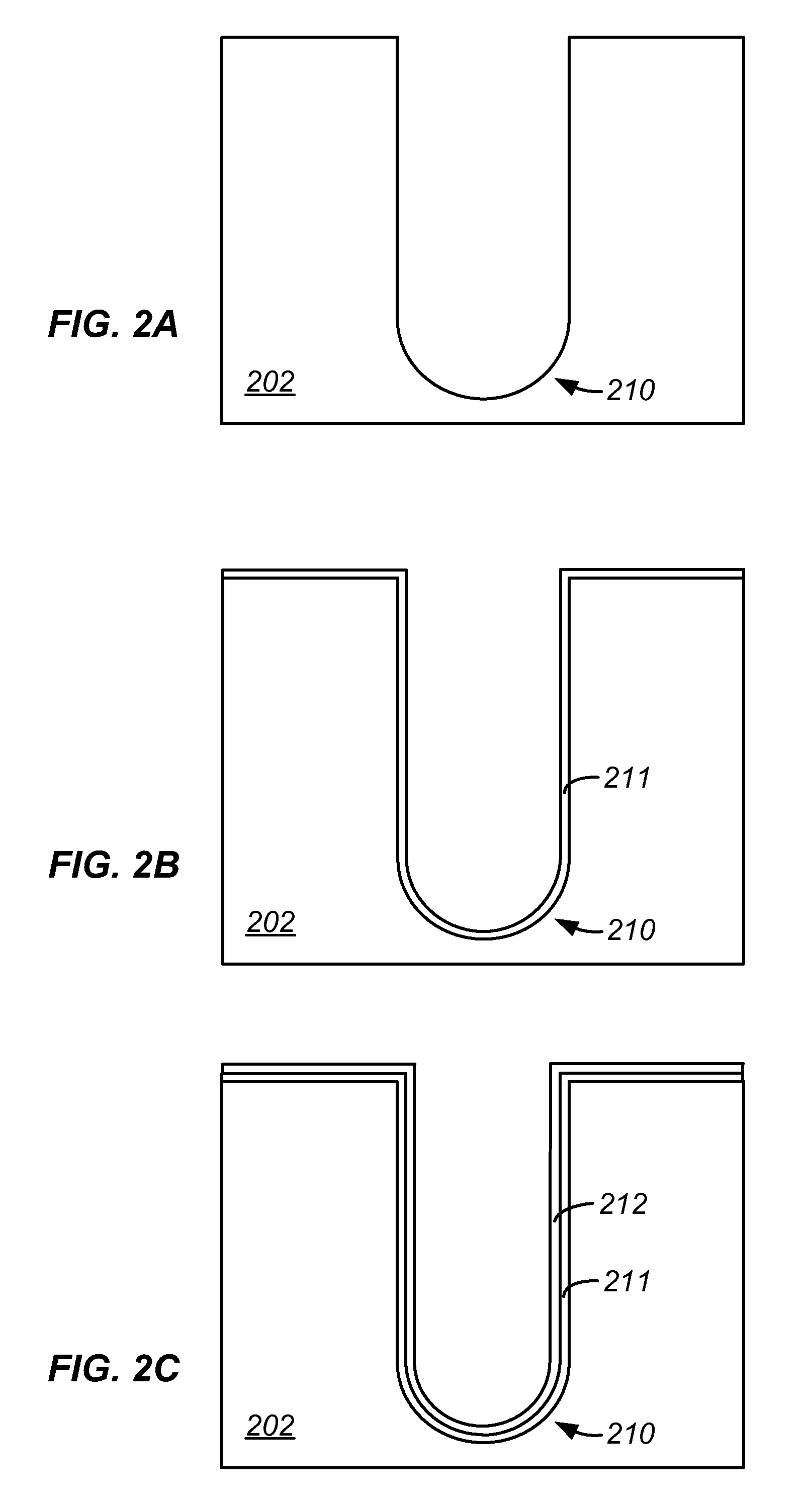
[0036]In accordance with embodiments of the invention, various techniques are described for forming inter-electrode dielectric (IED) and gate dielectric in shielded gate trench FETs. In one embodiment, a composite dielectric layer of nitride and oxide is used for protecting the surface of the trench sidewalls when the shield electrode is being oxidized to form the IED. High quality IED can be advantageously formed by thermal oxidation to a desired thickness. In one embodiment, the composite dielectric layer is used as the gate dielectric, which provides a barrier to mobile ions and moisture and also adds robustness to process defects. In one variation of the invention, a polysilicon liner is deposited and oxidized to reduce sharp recessed corners of the IED thereby substantially minimizing the electric field at bottom corners of the gate electrode. In alternate embodiments, techniques are provided for removing the nitride layer from the gate dielectric, which is desirable in applica...


PUM


Abstract

A shielded gate field effect transistor includes a trench extending into a semiconductor region. A shield electrode is in a lower portion of the trench, and is insulated from the semiconductor region by a shield dielectric. The shield dielectric comprises first and second dielectric layers, the first dielectric layer extending between the second dielectric layer and the semiconductor region. The second dielectric layer comprises a material which during oxidation process inhibits growth of oxide along surfaces of the semiconductor region covered by the second dielectric layer. An inter-electrode dielectric overlies the shield electrode, and a gate dielectric lines upper trench sidewalls. A gate electrode is in an upper portion of the trench over the inter-electrode dielectric.

Description

CROSS-REFERENCES TO RELATED APPLICATIONS[0001]This application claims the benefit of U.S. Provisional Application No. 60 / 956,980, filed Aug. 21, 2007, which is incorporated by reference in its entirety for all purposes.BACKGROUND OF THE INVENTION[0002]The present invention relates in general to semiconductor technology, and more particularly to methods and structures for forming inter-electrode dielectric and gate dielectric in shielded gate trench FETs.[0003]Shielded gate trench FETs are advantageous over conventional FETs in that the shield electrode reduces the gate-drain capacitance (Cgd) and improves the breakdown voltage of the transistor without sacrificing the transistor on-resistance. FIG. 1 is a simplified cross sectional view of a conventional shielded gate trench MOSFET. An n-type epitaxial layer 102 extends over n+ substrate 100. N+ source regions 108 and p+ heavy body regions 106 are formed in a p-type body region 104 which is in turn formed in epitaxial layer 102. Tre...

Claims


Application Information

Patent Timeline
Patent Type & Authority Applications(United States)
IPC IPC(8): H01L29/94H01L21/336
CPCH01L29/407H01L29/41766H01L29/7813H01L29/66734H01L29/66727H01L29/0669H01L29/42392H01L29/66621H01L29/78696H01L31/035281H01L33/18Y02E10/50H01L2029/42388H01L2924/0002H10N10/17
Inventor MADSON, GORDON K.
Owner SEMICON COMPONENTS IND LLC
Why Eureka
Try Eureka