Semiconductor sensor device and method for manufacturing same

a sensor device and semiconductor technology, applied in the field of semiconductor sensor devices, can solve the problems of high manufacturing cost of ceramic cases, difficult to make them smaller-sized but also lighter, and high thickness of the cas

Inactive Publication Date: 2009-02-26
HITACHI METALS LTD
View PDF3 Cites 41 Cited by
  • Summary
  • Abstract
  • Description
  • Claims
  • Application Information

AI Technical Summary

Benefits of technology

[0057]The semiconductor sensor device of the present invention employing wet-etching to cut the cap substrate to divide it into cap chips does not suffer from cracks in its cap chip and molding resin and can ensure airtightness betwe

Problems solved by technology

Since there is a limit to make the thickness of the case 71h and the case lid 72h thinner because they are made of ceramic, it is difficult to make them smaller-sized but also lighter.
Since the case terminals 74h and the outer terminals 75h are formed on the ceramic case 71h and they are connected t

Method used


Image

  • Semiconductor sensor device and method for manufacturing same
  • Semiconductor sensor device and method for manufacturing same
  • Semiconductor sensor device and method for manufacturing same

Examples


example 1

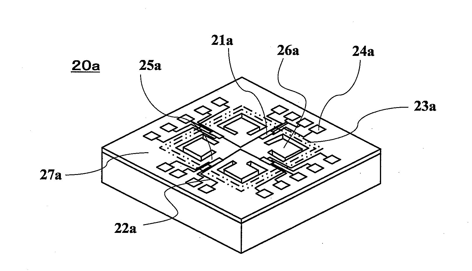
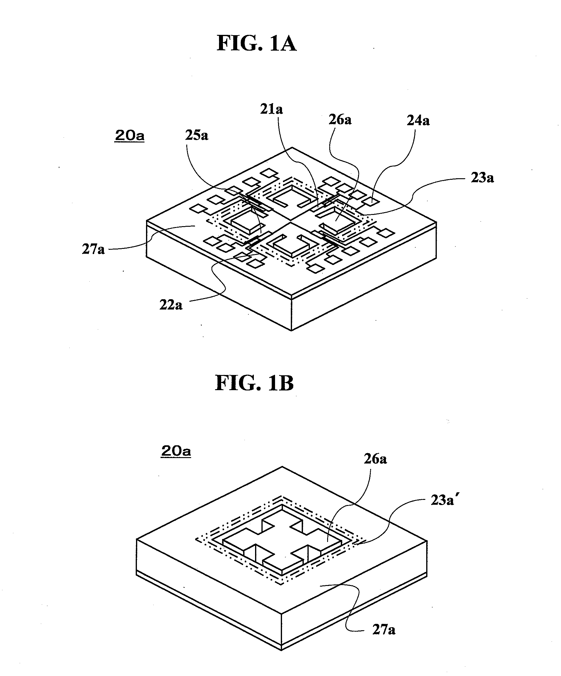
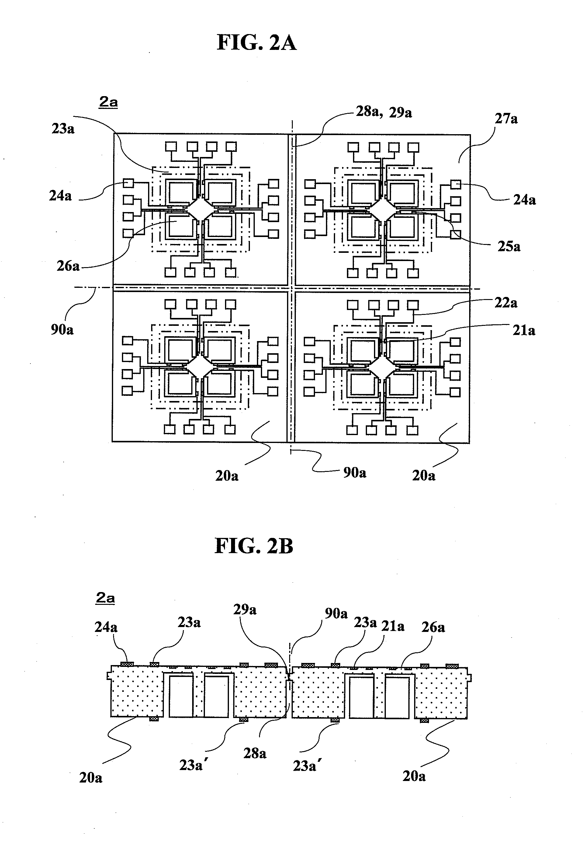
[0077]According to EXAMPLE 1 of the present invention, with reference to FIGS. 1 to 4, the structure of a semiconductor sensor device and a manufacturing process will be now described with an acceleration sensor device as an example. In the following description, a semiconductor sensor substrate and a semiconductor sensor chip manufactured by an MEMS technology are treated as synonymous with an acceleration sensor substrate and an acceleration sensor chip, respectively. FIGS. 1A and 1B are perspective views of a semiconductor sensor chip viewed from the top and the bottom, respectively; FIGS. 2A and 2B are a plan view and a cross-sectional view of the semiconductor sensor substrate, respectively; FIGS. 3A and 3B are a plan view and a cross-sectional view of the cap substrate, respectively; and FIGS. 4A to 4G are explanatory views of a manufacturing process of the semiconductor sensor device.

[0078]As shown in FIGS. 1A and 1B, a semiconductor sensor chip (acceleration sensor chip) 20a...

example 2

[0088]With reference to FIGS. 5 and 6, a semiconductor sensor device (acceleration sensor device) in EXAMPLE 2 of the present invention will be described. FIG. 5 partially illustrates the semiconductor sensor substrate (acceleration sensor substrate) 2b. FIG. 5A is a plan view of the semiconductor sensor substrate 2b on the side having piezo-resistors 21b; and FIG. 5B is a cross-sectional view of FIG. 5A. FIGS. 6A to 6G are explanatory views of a manufacturing process of the semiconductor sensor device 10b of EXAMPLE 2. The semiconductor sensor substrate 2b in FIG. 5 has the same structure and components as the semiconductor sensor substrate of EXAMPLE 1 except for the lack of dividing gutters 28a and couplings 29a, which are provided in the semiconductor sensor substrate of EXAMPLE 1, and therefore its detailed description will be omitted. The shape and material of cap substrates 3b, 3b′ were also the same as those of the cap substrate 3a in EXAMPLE 1.

[0089]The manufacturing proces...

example 3

[0091]Cap chips of EXAMPLE 3 having a crystal orientation different from the cap chips of EXAMPLES 1 and 2 were thinned and divided by wet-etching, while a semiconductor sensor substrate was cut by a cutting wheel to obtain semiconductor sensor chips. With reference to FIG. 7, a description will be made about a manufacturing process of the semiconductor sensor device (acceleration sensor device) of EXAMPLE 3. FIG. 7A is a plan view of a cap substrate 3c or 3c′ viewed from the side to be bonded to a semiconductor sensor substrate (acceleration sensor substrate) 2c; and FIG. 7B is a cross-sectional view of FIG. 7A. Each side surface of the cap substrates 3c, 3c′ was composed of a {100} silicon crystal plane. Drive suppression grooves 31c facing weights of the semiconductor sensor substrate are octagons each surrounded by {100} planes and {111} planes and having edge portions 311c rounded off by over-etching, namely obtuse edges. Outside edge portions 312c corresponding with the edge p...


PUM


Abstract

Provided is a semiconductor sensor device which is manufactured by an MEMS technology wherein machining technology and/or material technology is combined with semiconductor technology for detecting and measuring various physical quantities. In the semiconductor sensor device, cracks which generate in a cap chip and a molding resin are eliminated and air-tightness between a semiconductor sensor chip and the cap chip is ensured. The cracks due to vibration applied when being cut can be eliminated by having the circumference side surface of the cap chip as a wet-etched surface. Furthermore, insulation is ensured by coating the cap chip side surface with an insulating protection film.

Description

TECHNICAL FIELD[0001]The present invention relates to a semiconductor sensor device having an MEMS (Micro-Electro-Mechanical Systems) chip and a method for manufacturing it, in particular to a semiconductor sensor device provided with an MEMS chip having a movable part and a manufacture of it.BACKGROUND ART[0002]The MEMS technology, in which semiconductor manufacturing process technologies are incorporated with mechanically machining technologies and / or material technology to realize a system having a fine three-dimensional structure on a semiconductor substrate, can be applied to a wide variety of fields. Applications of semiconductor sensor devices manufactured by the MEMS technology to detections of physical quantities, such as acceleration, angular velocity, pressure, in fields of automobiles, aero planes, mobile terminal devices and toys, particularly attract attention from people.[0003]These semiconductor sensor devices have a special feature in having a movable part formed by...

Claims


Application Information

Patent Timeline
IPC IPC(8): H01L29/84H01L21/58
CPCB81C1/00873G01C19/5719H01L2924/1461H01L2224/45144H01L2224/48145H01L2224/48091G01P15/18G01P1/023G01P15/0802G01P15/123G01P15/125H01L2924/00014H01L2924/00H01L2224/73265H01L2924/00012H01L23/02H01L23/28H10N30/88
Inventor AONO, TAKANORIOKADA, RYOJIKAZAMA, ATSUSHITAKADA, YOSHIAKI
Owner HITACHI METALS LTD
Why Eureka
Try Eureka