Wafer transfer apparatus, wafer transfer method and storage medium

a technology of wafer detection and storage medium, which is applied in the directions of pile separation, transportation and packaging, instruments, etc., can solve the problems of excessive force to act on the wafer, wafers will collide with the chamber wall, and the wafers will be difficult to locate, so as to achieve a processing system at a low cost and facilitate the layout of wafer detection sensors.

Active Publication Date: 2009-02-26
TOKYO ELECTRON LTD
View PDF11 Cites 332 Cited by
  • Summary
  • Abstract
  • Description
  • Claims
  • Application Information

AI Technical Summary

Benefits of technology

[0022]According to one aspect of the present invention, the position of a wafer mounted on the transfer arm is detected using one wafer detection sensor adapted to judge whether or not the wafer is passing therethrough. Therefore, it is possible to make a processing system at a low cost, and to easily layout the wafer detection sensors. In addition, according to another aspect of the present invention, since calculations are made in consideration of a correct diameter of the wafer which is determined based on wafer periphery data obtained when the orientation of the wafer is detected, it is possible to precisely determine the position of the center of the wafer.

Problems solved by technology

When a wafer is transferred from the alignment mechanism to the process chamber, there is a possibility that, for example, a malfunction of a transfer arm will cause a positional deviation of the wafer.
In addition, when a processed wafer is removed from an electrostatic chuck, there is also a possibility that a residual electric charge may cause excessive force to act on the wafer to displace the wafer.
If the wafer displaces from its proper position on the transfer arm, when the wafer passes through a transfer port of a process chamber and that of a load lock chamber, there is a possibility that the wafer will collide with the chamber wall.
Moreover, in the case of a wafer before processed, even if the wafer is carried into the process chamber, the wafer is not correctly mounted on a mounting table.
Therefore, it is not possible to ensure the in-plane uniformity of the process.
However, since the foregoing sensors configured to detect the wafer position when the transfer arm is stopped is expensive, the provision of plural monitoring areas leads to increase in the total cost of the system.
In addition, in a case where plural sensors are provided in one monitoring area and plural monitoring areas are provided in a system, the layout of the sensors becomes difficult.
Moreover, if the number of sensors is large, it is possible that the positional relationship between the sensors is not accurate.
Inaccurate positional relationship between the sensors will result in an error in calculating the center position of the wafer.
However, this technique cannot solve the foregoing problems.

Method used


Image

  • Wafer transfer apparatus, wafer transfer method and storage medium
  • Wafer transfer apparatus, wafer transfer method and storage medium
  • Wafer transfer apparatus, wafer transfer method and storage medium

Examples


Embodiment Construction

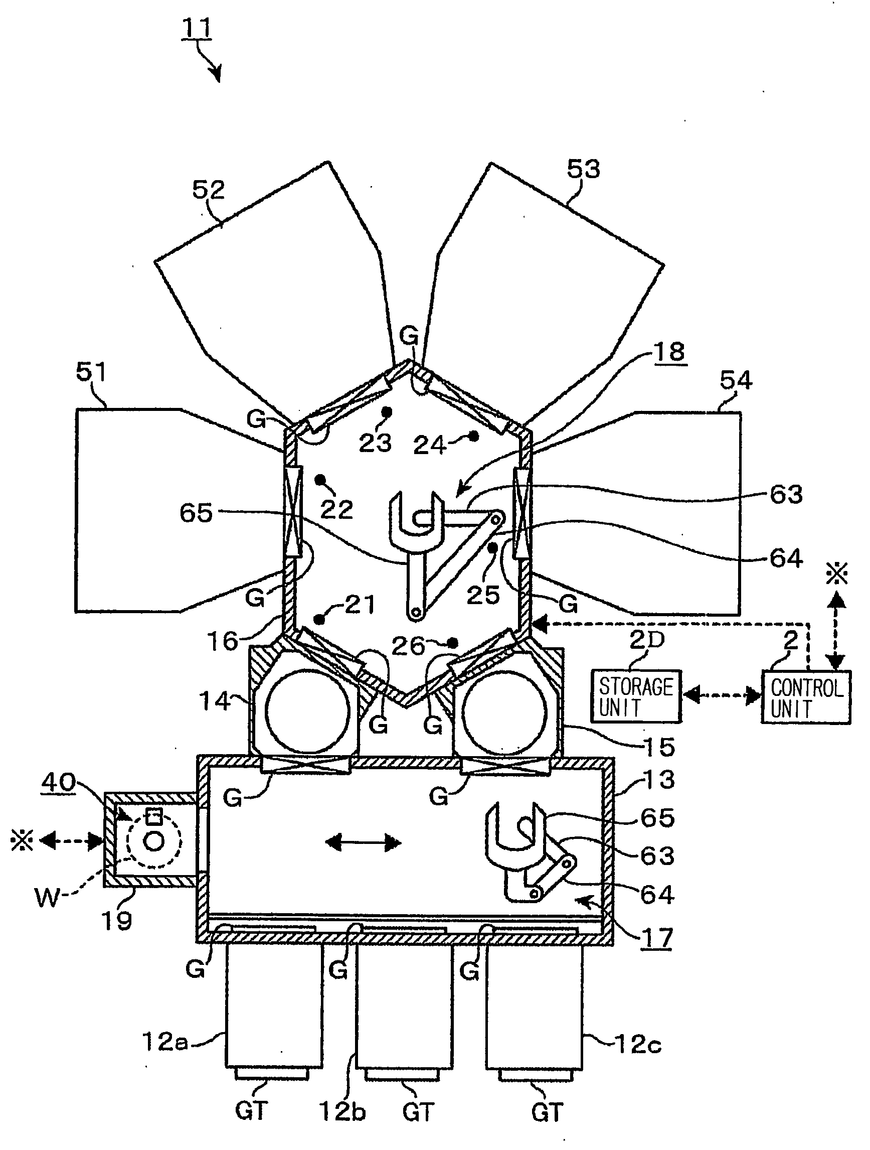
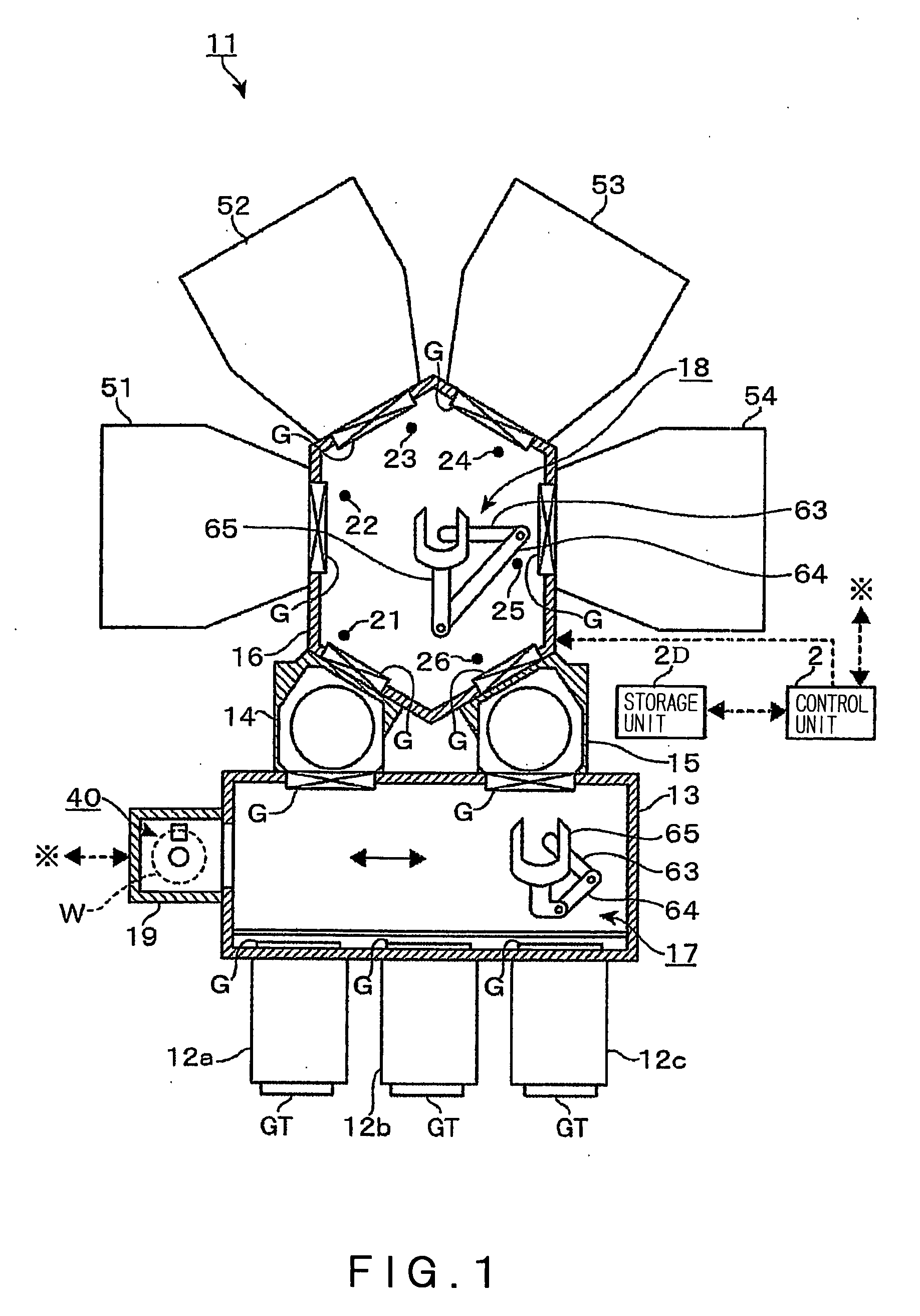
[0034]An example of a substrate processing system including a wafer transfer apparatus according to the present invention will be described with reference to FIG. 1. The substrate processing system 11 shown in FIG. 1 is generally called a cluster tool, a multi-chamber system, or the like. The substrate processing system 11 includes: carrier chambers 12a, 12b and 12c; a first transfer chamber 13, load lock chambers 14 and 15; a second transfer chamber 16; processing units (processing chambers) 51, 52, 53 and 54; and gate valves G for opening / closing each of the chambers (for simplicity, the same reference sign G is given to those gate valves). An alignment unit 19 is mounted to a side of the first transfer chamber 13. The alignment unit 19 houses an alignment mechanism 40 described later. Each of the load lock chambers 14 and 15 is provided with a vacuum pump and a leak valve (which are not shown) so that a wafer W can be transferred, through the load lock chamber 14 or 15, between t...


PUM


Abstract

One sensor constituted of a light emission element and a light-receiving element is provided in a path through which a wafer is transferred. The sensor is positioned so that the wafer passes through an area between the light emission element and the light-receiving element. Coordinates of the center of the wafer are calculated based on encoder values obtained when the wafer starts passing through the sensor and when the wafer completes passing through the sensor, position data of wafer transfer means corresponding to the encoder value, and the diameter of the wafer; and thereby the amount of positional deviation of the center of the wafer from a reference position is calculated.

Description

CROSS REFERENCE TO RELATED APPLICATION[0001]The present application claims the benefit of U.S. provisional application No. 60 / 844,651, which is incorporated herein by reference in its entirety.TECHNICAL FIELD[0002]The present invention relates to a technique for measuring the positional deviation a wafer mounted on transfer means in a transfer apparatus for transferring the wafer.BACKGROUND ART[0003]When a wafer is processed in a semiconductor manufacturing system, the orientation of the wafer is typically aligned by an alignment mechanism in advance on the basis of a notch (V-shaped slit indicating a reference direction corresponding to the direction of a crystal array of the wafer). The alignment mechanism mounts the wafer on its rotatable stage, and rotates the wafer by 3600 or more, and then detects the direction of the wafer on the basis of obtained data of the peripheral edge of the wafer. In this case, the alignment mechanism usually adopts a method that pushes the wafer at, ...

Claims


Application Information

Patent Timeline
Patent Type & Authority Applications(United States)
IPC IPC(8): H01L21/677
CPCH01L21/681H01L21/67748Y10S414/136
Inventor WAKABAYASHI, SHINJI
Owner TOKYO ELECTRON LTD
Why Eureka
Try Eureka