Cleaving Wafers from Silicon Crystals

a technology of silicon crystals and thin wafers, which is applied in the field of cleaving thin wafers from single-crystal silicon ingots, can solve problems such as crystal fracture, and achieve the effect of efficient absorbing

Active Publication Date: 2009-03-05
BAER
View PDF21 Cites 86 Cited by
  • Summary
  • Abstract
  • Description
  • Claims
  • Application Information

AI Technical Summary

Benefits of technology

[0018]An ingot of single-crystal silicon with a (111) axis is flattened and polished at one end normal to the axis, and a notch with a vertex in the (111) plane is produced on a side of the ingot, such that the distance between this vertex and said end is the desired thickness of a wafer to be cleaved from the ingot and such this vertex is in the desired plane of cleavage. Light of a wavelength able to penetrate into the silicon crystal without significant absorption, when the intensity of the beam is low, but is efficiently absorbed and converted to heat when the intensity of the beam is high...

Problems solved by technology

Heating and the resulting transient local expansion of the silicon in this illuminated volume causes tensile stress at the vertex ...

Method used


Image

  • Cleaving Wafers from Silicon Crystals
  • Cleaving Wafers from Silicon Crystals
  • Cleaving Wafers from Silicon Crystals

Examples


Embodiment Construction

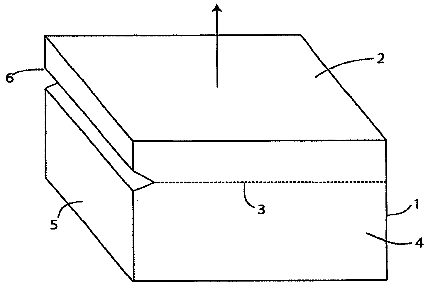
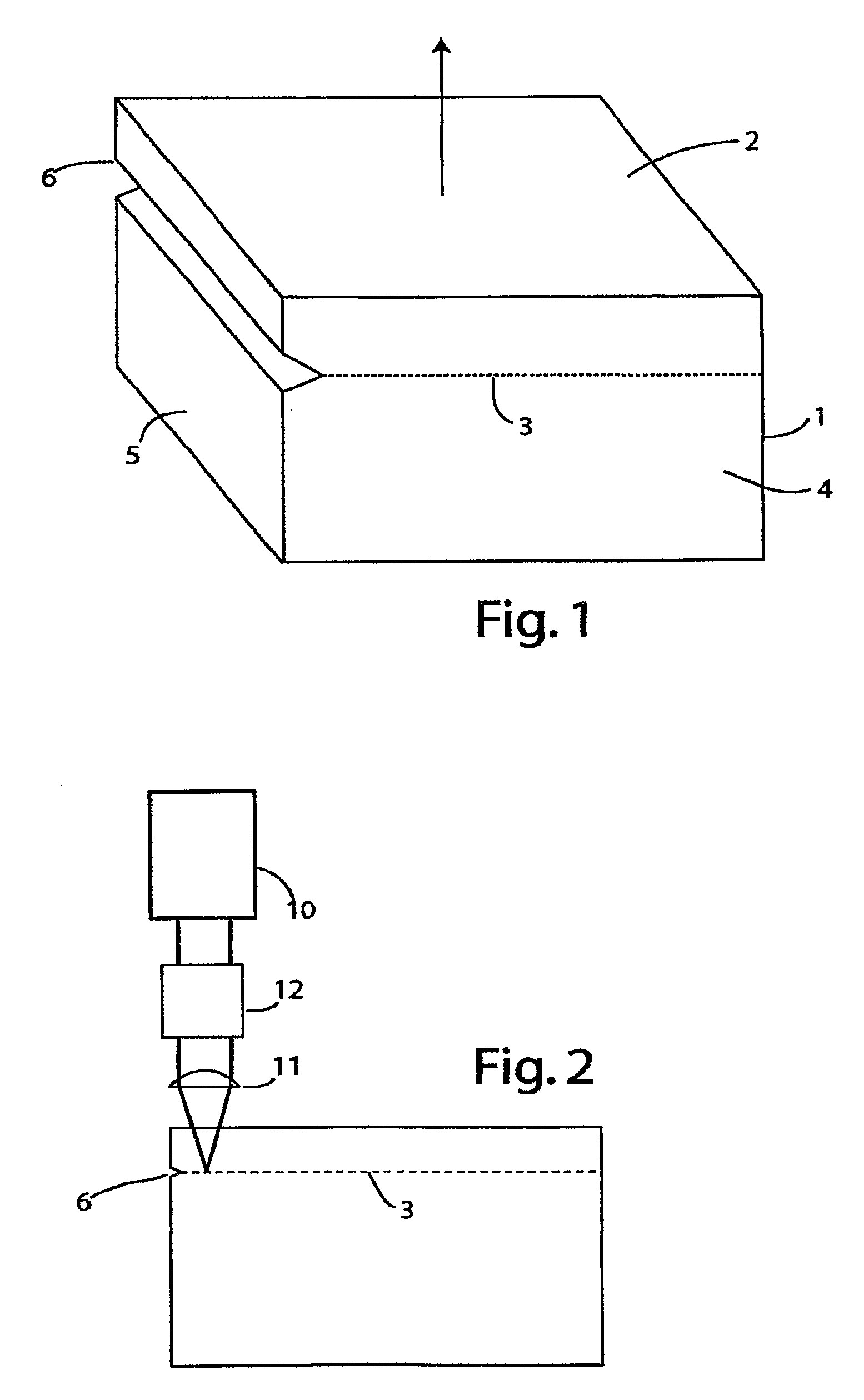
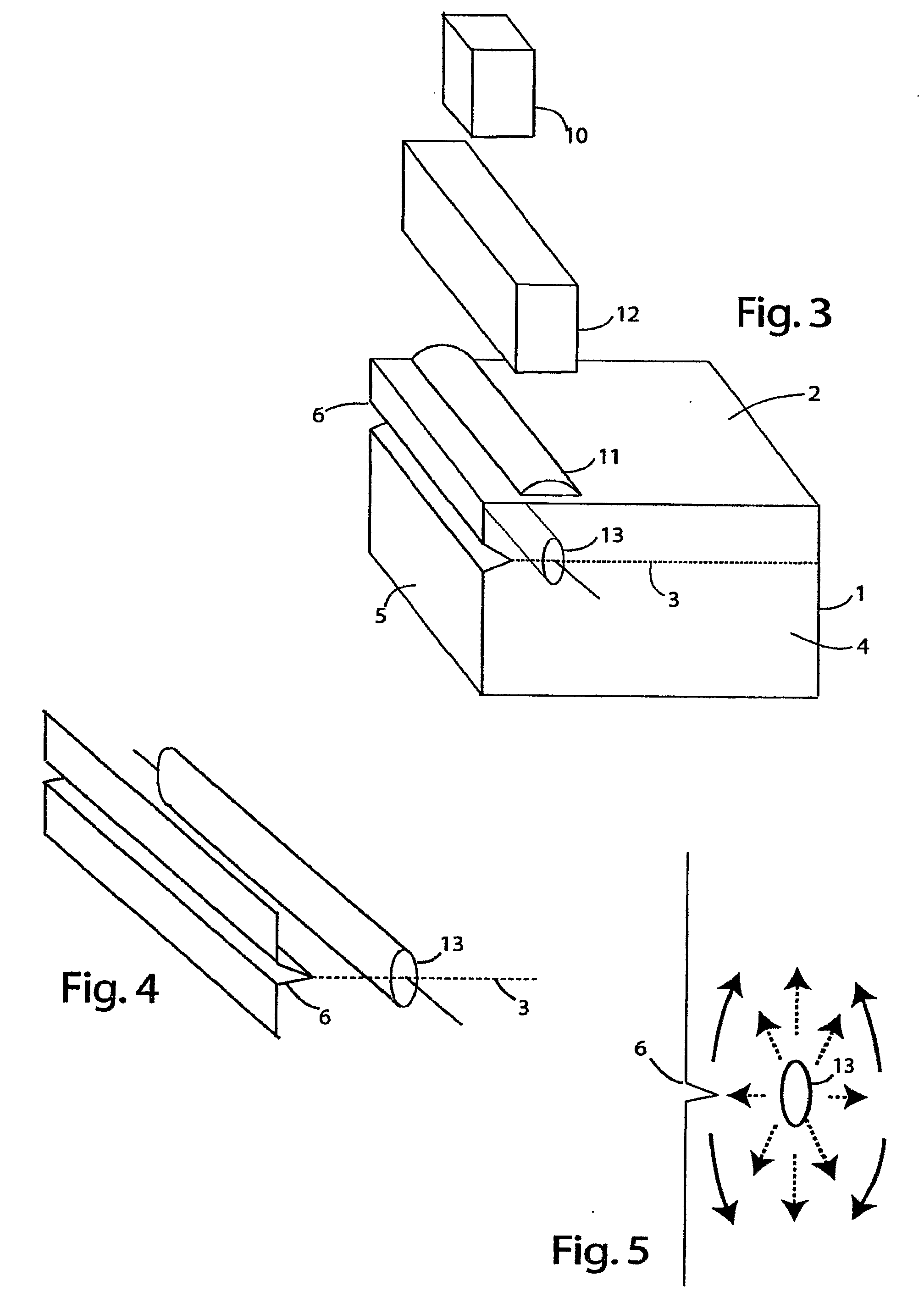
[0036]FIG. 1 shows an ingot 1 of single-crystal silicon. To simplify the present discussion, ingot 1 has been ground to a rectangular prism shape. One face 2 of the ingot, normal to the main crystal axis (identified by an arrow), is ground and polished, and will serve as one face of the first wafer to be cleaved from the ingot by the method of the present invention. The desired cleavage plane is parallel to face 2 and is shown by the dotted line 3 where it intersects a face 4 of ingot 1 perpendicular to face 2. On another face 5 of ingot 1, perpendicular to both faces 2 and 4, is a notch 6 with a vertex in the desired cleavage plane. Since the (111) plane is the cleavage plane of silicon, the main axis of ingot 1 is oriented in the (111) direction. In practice, in order to maximize utilization of the fill cross sectional area of the silicon ingot, the ingot might be left in its existing cylindrical shape, with notch 6 produced on one side. Furthermore, the ideal location of the notc...


PUM

PropertyMeasurementUnit
Wavelengthaaaaaaaaaa
Temperatureaaaaaaaaaa

Abstract

A method of creating thin wafers of single crystal silicon wherein an ingot of single-crystal silicon with a (111) axis is flattened and polished at one end normal to the axis, and a notch with a vertex in the (111) plane is produced on a side or edge of the ingot, such that the distance between this vertex and said end is the desired thickness of a wafer to be cleaved from the ingot and such this vertex is in the desired plane of cleavage. Light of a wavelength able to penetrate into the silicon crystal without significant absorption, when the intensity of the beam is low, but is efficiently absorbed and converted to heat when the intensity of the beam is high, is focused to an elongated volume with an axis of elongation in the desired cleavage plane, parallel to and a short distance from said notch edge. Heating and the resulting transient local expansion of the silicon in this illuminated volume causes tensile stress at the vertex of said notch, substantially normal to the desired cleavage plane, thereby causing fracture of the crystal in the chosen cleavage plane. Movement of the illuminated volume relative to the ingot allows the fracture to propagate across the desired cleavage plane, thereby completely severing the wafer from the rest of the ingot.

Description

CROSS REFERENCE TO RELATED APPLICATIONS[0001]This application claims priority from U.S. Provisional Patent Application Ser. No. 60 / 761,547 filed Jan. 24, 2006, from U.S. Provisional Patent Application Ser. No. 60 / 745,035 filed Apr. 18, 2006, from U.S. Provisional Patent Application Ser. No. 60 / 745,759 filed Apr. 27, 2006, and from U.S. Provisional Patent Application Ser. No. 60 / 808,553 filed Jul. 5, 2006, the entire disclosures of which are hereby incorporated by reference.FIELD OF THE INVENTION[0002]The present invention relates to silicon wafer technology, and in particular to the problem of cleaving thin wafers from ingots of single-crystal silicon.DESCRIPTION OF THE PRIOR ART[0003]Most photovoltaic solar cells produced today are based on crystalline silicon, either single-crystal silicon or polycrystalline silicon. The single-crystal silicon cells convert solar energy more efficiently, but are more expensive. Because the cost of the silicon substrate is currently a major compone...

Claims


Application Information

Patent Timeline
IPC IPC(8): H01L21/00C01B33/02B26D7/10B26D5/06
CPCB23K26/0057B28D5/0011B28D1/221B23K26/4075B23K26/40C30B29/06C30B33/06B23K2103/50Y10T83/141Y10T83/041B23K26/53
Inventor BAER
Owner BAER
Why Eureka
Try Eureka