Shielding member of processing system

a technology of shielding member and processing system, which is applied in the direction of electric shock equipment, vacuum evaporation coating, coating, etc., can solve the problems of affecting the processing efficiency affecting the effect of the shielding member, so as to reduce the thickness of the adhesion promoter layer, reduce the chance of arcing, and increase the processing time

Inactive Publication Date: 2009-03-05
UNITED MICROELECTRONICS CORP
View PDF6 Cites 5 Cited by
  • Summary
  • Abstract
  • Description
  • Claims
  • Application Information

AI Technical Summary

Benefits of technology

[0019]Since the thickness of the adhesion promoter layer of the present invention is reduced at a region of the shielding member in close proximity to the target, the problem of peeling of the adhesion promoter layer from the base metal is mitigated. Further, by reducing the thickness of the adhesion promoter layer in the region of the shielding member in close proximity to the target layer

Problems solved by technology

However, it has been observed that after several deposition cycles, the coating material at the top region of the shielding member near the target tends to peel off or shed from the surface of the base metal.
Once particles are generated in the chamber due to the peeling of the coating material, they may become incorporated into the gro

Method used


Image

  • Shielding member of processing system
  • Shielding member of processing system

Examples


Embodiment Construction

[0024]Reference will now be made in detail to the embodiments of the invention, examples of which are illustrated in the accompanying drawings. Whenever possible, the same reference numbers are used in the both FIG. 1 and FIG. 2 of the drawings and the description to refer to the same or like parts.

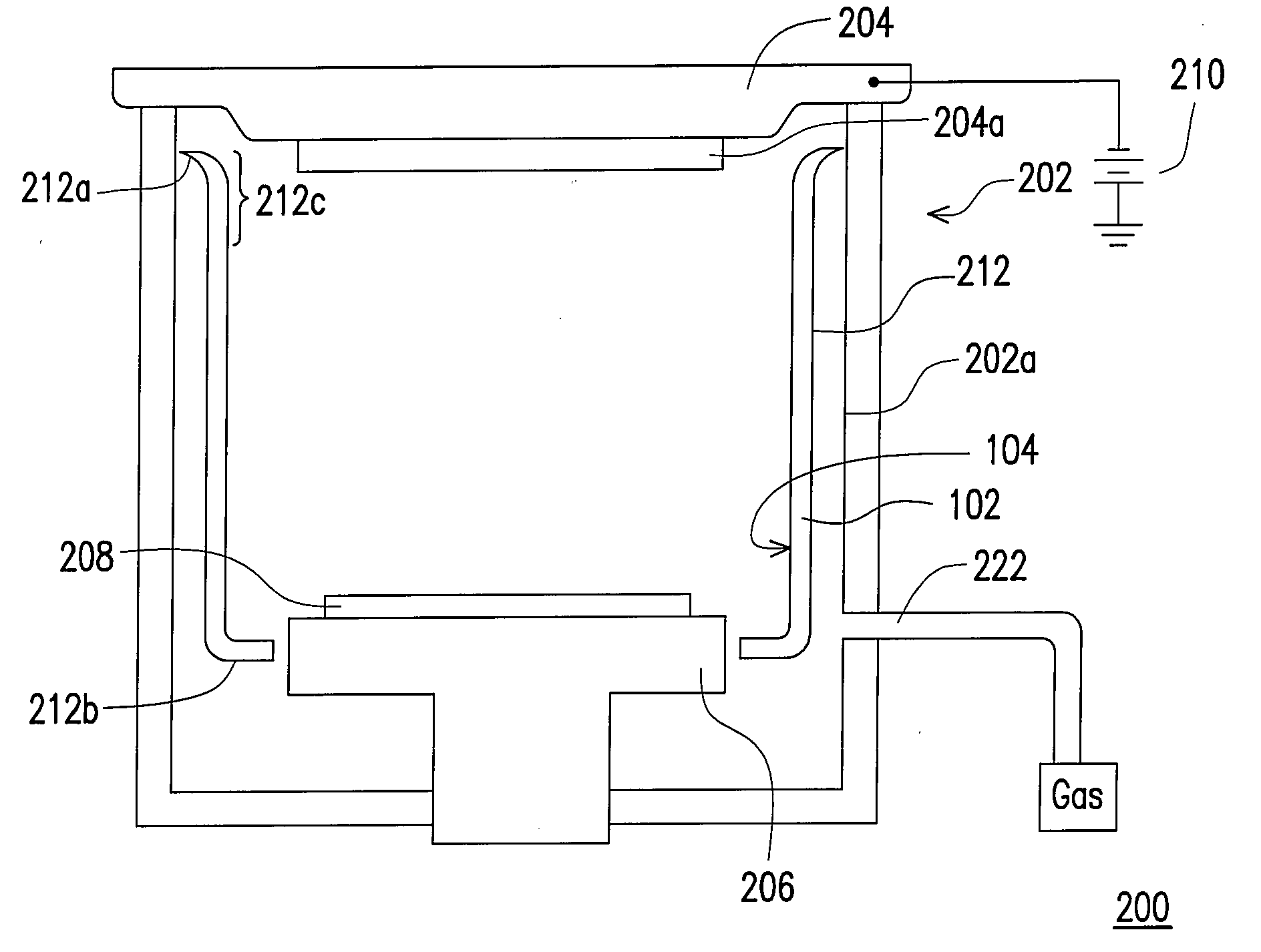
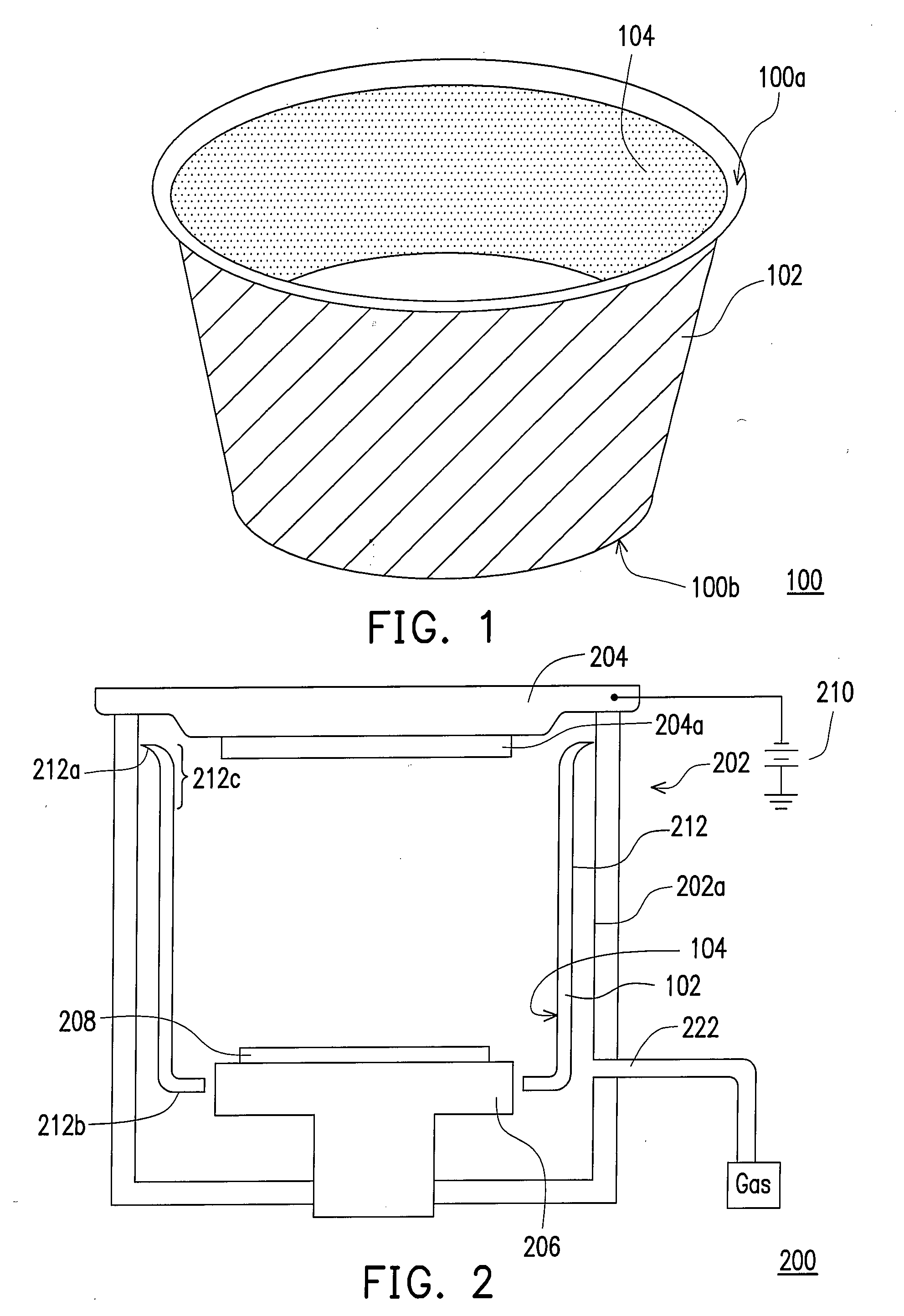
[0025]Referring to FIG. 1, wherein FIG. 1 is a diagram of a shielding member fabricated according to one embodiment of the invention. The shielding member 100 of the invention is, for example, an inner shield formed to cover the inner surface of a processing apparatus, such as a physical vapor deposition chamber. The shielding member 100 is, for example, an annular plate that may or may not include a bottom plate. The shielding member 100 includes two distinct ends: a first end 100a and a second end 100b. In the case that the shielding member 100 is applied as an inner shield in a physical vapor deposition apparatus, the first end 100a is positioned substantially adjacent to a target laye...


PUM

PropertyMeasurementUnit
Lengthaaaaaaaaaa
Lengthaaaaaaaaaa
Fractionaaaaaaaaaa

Abstract

A shielding member applicable in a deposition apparatus is provided. The shielding member includes a base metal and an adhesion promoter layer arc-sprayed on the base metal, wherein adhesion promoter layer has a thickness gradient increasing from an upper end of the shielding member to a lower end of the shielding member. More preferably, no adhesion promoter layer is formed in the upper 10 cm of the shielding member, adjacent to a target layer.

Description

BACKGROUND OF THE INVENTION[0001]1. Field of Invention[0002]The present invention relates to a shielding member of a processing system; more specifically, the present invention is related to an inner shield applicable in a sputtering chamber of a physical vapor deposition (PVD) processing system and a method of forming the shield.[0003]2. Description of Related Art[0004]Physical vapor deposition, also known as sputtering, is the most established method of depositing metal layers in the fabrication of semiconductor devices. A sputter reactor chamber is typically arranged with a target being supported on the vacuum sealed chamber and a heater supporting a wafer to be sputtered in a position opposite to that of the target. The target is composed of metal or metal compound to be sputtered, for example, tantalum or nickel-platinum. The sputter reactor chamber normally includes a shielding member, for example, an inner shield, to prevent the sputter material from coating. Instead, the spu...

Claims


Application Information

Patent Timeline
IPC IPC(8): B05C11/11
CPCC23C14/564C23C4/105C23C4/11
Inventor LOO, CHEE-MONGLIU, YAO-HUNG
Owner UNITED MICROELECTRONICS CORP
Why Eureka
Try Eureka