Wiring substrate with lead pin and lead pin
- Summary
- Abstract
- Description
- Claims
- Application Information
AI Technical Summary
Benefits of technology
Problems solved by technology
Method used
Image
Examples
Embodiment Construction
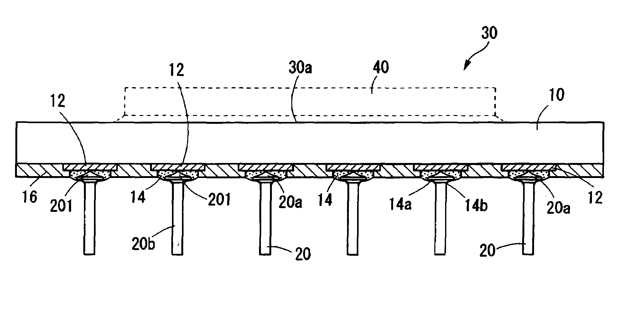
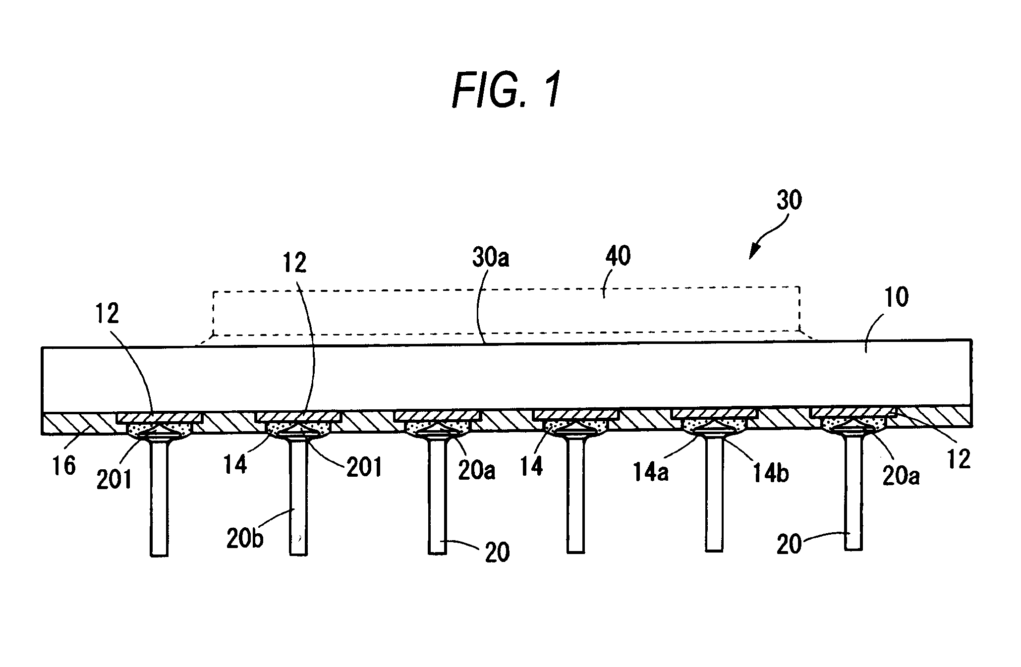
[0035]FIG. 1 is a sectional view showing a configuration of one embodiment of a wiring substrate with lead pins according to the invention. A wiring substrate 30 with lead pins of the present embodiment is formed by disposing an installation part 30a for installing a semiconductor element 40 on one surface of a wiring substrate 10 and forming electrode pads 12 on the other surface of the wiring substrate 10 and bonding lead pins 20 to the electrode pads 12 by conductive materials 14 made of tin-antimony alloys.
[0036]A necessary wiring pattern and a pad for connection electrically connected to the semiconductor element 40 are formed in the installation part 30a. The other surface of the wiring substrate 10 is covered with a protective film 16 such as a solder resist, and the electrode pad 12 to which the lead pin 20 is bonded is exposed in a circular plane shape. The electrode pad 12 is formed by a copper layer, and nickel plating and gold plating are given to a surface of the copper...
PUM
 Abstract
Description
Claims
Application Information


