Bipolar device and fabrication method thereof

a bipolar device and fabrication method technology, applied in the direction of basic electric elements, semiconductor devices, electrical apparatus, etc., can solve the problems of difficulty in improving the switching frequency, and inability to ensure the required current gain 35 for practical use, etc., to achieve good reproducibility and controllability, reduce the size and increase the frequency, and achieve sufficient current gain

Inactive Publication Date: 2009-03-05
HITACHI LTD
View PDF2 Cites 33 Cited by
  • Summary
  • Abstract
  • Description
  • Claims
  • Application Information

AI Technical Summary

Benefits of technology

[0018]According to the invention, reduction in the size and increased in the frequency can be attained in the bipolar device. Further, the structure can be attained at good reproducibility and controllability.
[0019]That is, the invention can at first provide a bipolar transistor capable of ensuring a practically sufficient current gain and suitable for size-reduction.
[0020]Secondly, the invention can provide a thyristor capable of high frequency switching at a low turn-on loss.
[0021]Thirdly, the invention can provide a bipolar transistor having an extremely high current gain in which the power dissipation in the base drive circuit is decreased to a not negligible level.

Problems solved by technology

As a result, in a bipolar transistor, emitter size dependence of the current gain occurs, and a problem that the current gain of 35 required for practical use cannot be ensured arises when the emitter is made finer to less than existent 12 μm or so.
Further, in the thyristor, since the gate current upon turn-on is large, and the turn-on loss reaches a not negligible level to DC loss when switching frequency is increased to 1 kHz or higher, improvement of the switching frequency is difficult.
Accordingly, when the emitter is refined from about 10 μm, there is a problem that a required current gain 35 for practical use cannot be ensured.
Further, in the thyristor, since the turn-on gate current is large and the turn-on loss is at an innegligible level to the DC loss when the switching frequency is increased to 1 kHz or higher, improvement of the switching frequency is difficult.

Method used


Image

  • Bipolar device and fabrication method thereof
  • Bipolar device and fabrication method thereof
  • Bipolar device and fabrication method thereof

Examples


embodiment 1

[0081]An npn type SiC bipolar transistor as a first embodiment of the invention and fabrication steps thereof are to be described with reference to FIG. 1, FIG. 7 to FIG. 11, and FIG. 23.

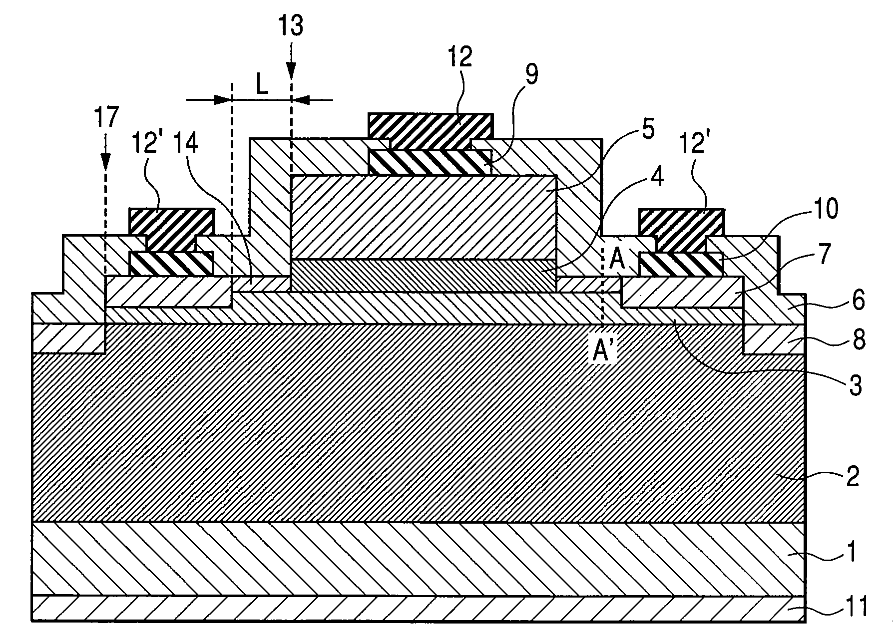
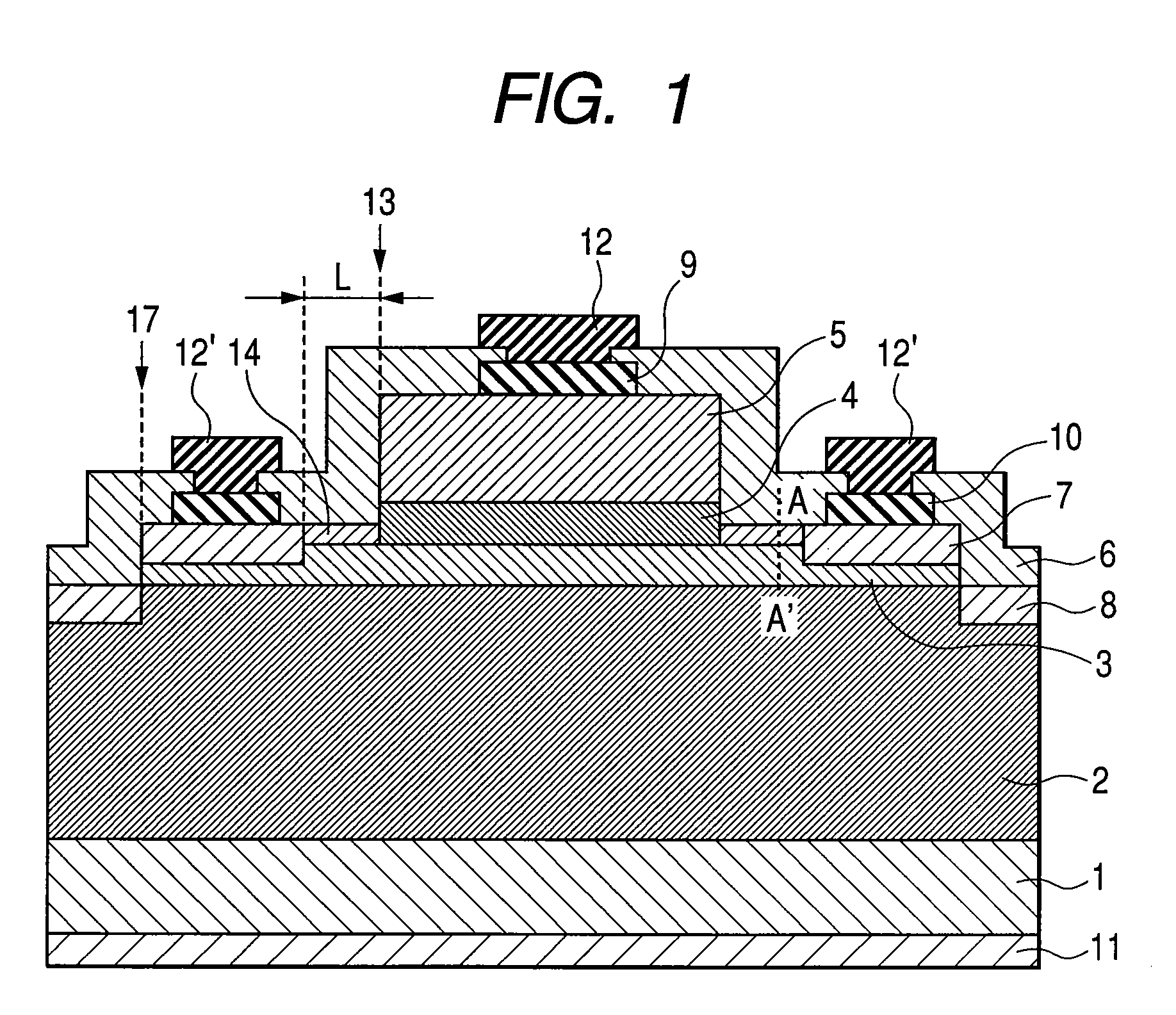
[0082]FIG. 1 is a vertical cross sectional structural view of an npn-type SiC bipolar transistor as a first embodiment of the invention, and FIG. 23 is a plan view thereof. Reference numerals are used in common with both of the drawings. Above an n-type SiC substrate 1 ((0001) Si surface, donor (N) density of 3×1018 cm−3), a collector layer 2 comprising an n-type SiC (15 μm thickness, donor (N) density: 2×1016 cm−3), a base layer 3 comprising a p-type SiC (1 μm thickness, acceptor (Al) density: 2×1017 cm−3), a first emitter layer 4 comprising an n-type SiC (100 nm thickness, donor (N) density: 3×1017 cm−3), and a second emitter layer 5 comprising an n-type SiC (1 μm thickness, donor (N) density: 1×1019 cm−3). Then, the second emitter layer 5, the first emitter layer 4 and the base layer 3 form a mes...

embodiment 2

[0093]An SiC thyristor and fabrication steps thereof as a second embodiment of the invention are to be described with reference to FIG. 2 and FIG. 12 to FIG. 16.

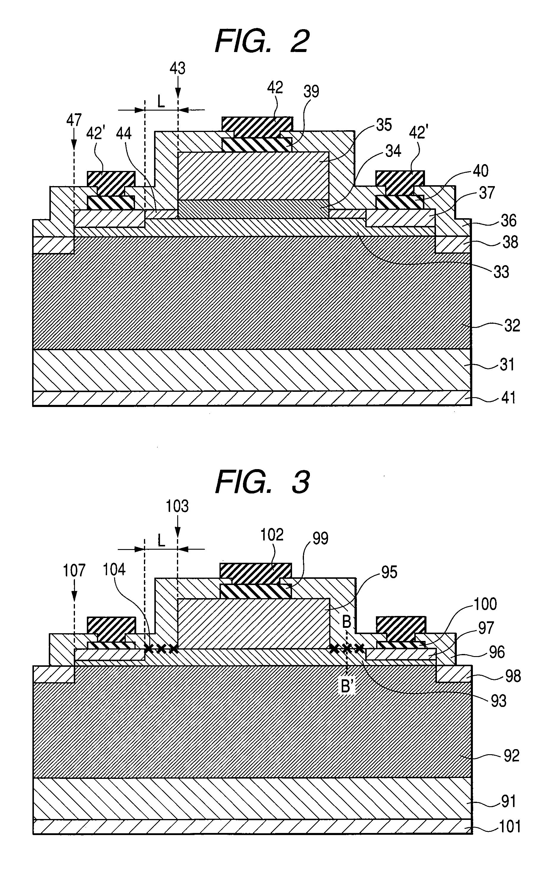
[0094]FIG. 2 is a vertical cross sectional vertical view of an SiC thyristor as a second embodiment of the invention. Above an n-type SiC substrate ((0001) Si surface, donor (N) density: 3×1018 cm−3) 31, a drift layer 32 comprising a p-type SiC (100 μm thickness, acceptor (Al) density; 2×1014 cm−3) layer, a gate layer 33 comprising an n-type SiC (1 μm thickness, donor (N) density: 2×1017 cm−3), a first anode layer 34 comprising a p-type SiC (100 nm thickness, acceptor (Al) density: 3×1017 cm−3), and a second anode layer 35 comprising a p-type SiC (1 μm thickness, acceptor (Al) density 1×1019 cm−3) are formed. Then, the second anode layer 35, the first anode layer 34, and the gate layer 33 form a mesa structure 43. Further, as the ohmic electrodes, an anode electrode (Ti / Al) 39 is formed directly to the second anode layer 35,...

embodiment 3

[0105]An npn-type SiC bipolar transistor and fabrication steps thereof as a third embodiment of the invention are to be described with reference to FIG. 17 to FIG. 23 and FIG. 29.

[0106]FIG. 22 is a vertical cross sectional structural view of an npn-type SiC bipolar transistor as a third embodiment of the invention, FIG. 23 is a plan view thereof, and FIG. 29 is a schematic band diagram at D-D′ section in FIG. 22. Above an n-type SiC substrate 51 ((0001) Si surface, donor (N) density: 3×1018 cm−3), a collector layer 52 comprising an n-type SiC layer (15 μm thickness, donor (N) density: 2×1016 cm−3), a base layer 53 comprising a p-type SiC (1 μm thickness, acceptor (Al) density: 2×1017 cm−3), a first emitter layer 54 comprising an n-type SiC (thickness: 100 nm, donor (N) density: 3×1017 cm−3), a second emitter layer 55 comprising an n-type SiC (15 nm thickness, donor (N) density: 1×1019 cm−3), a hole barrier layer 63 comprising HfO2 (1 nm thickness), a conduction band discontinuity re...


PUM


Abstract

In a mesa type bipolar transistor or a thyristor, since carriers injected from an emitter layer or an anode layer to a base layer or a gate layer diffuse laterally and are recombined, reduction in the size and improvement for the switching frequency is difficult.
In the invention, the emitter layer or the anode layer is formed of two high-doped and low-doped layers, a semiconductor region for suppressing recombination comprising an identical semiconductor having an impurity density identical with that of the low-doped layer is present being in contact with a base layer or a gate layer and a surface passivation layer, and the width of the semiconductor region for suppressing recombination is defined equal with or longer than the diffusion length of the carrier. This provides an effect of attaining reduction in the size of the bipolar transistor or improvement of the switching frequency of the thyristor without deteriorating the performance. Further, this has an effect of greatly improving the current gain by successively stacking above the high-doped emitter layer of the bipolar transistor, a hole barrier layer, a conduction band discontinuity relaxed layer and an emitter contact layer.

Description

CLAIM OF PRIORITY[0001]The present application claims priority from Japanese patent application JP 2007-222455 filed on Aug. 29, 2007, the content of which is hereby incorporated by reference into this application.FIELD OF THE INVENTION [0002]The present invention relates to a bipolar device typically represented by a bipolar transistor and a thyristor. The bipolar device of the present application is useful, particularly, for a power bipolar device of a reduced sized or capable of high frequency switching.BACKGROUND OF THE INVENTION [0003]In an existent power bipolar transistor for power application use, SiC is used as a semiconductor material, and a collector layer, a base layer and an emitter layer are arranged, for example, as shown in FIG. 3. FIG. 3 as a typical example is a vertical cross sectional structural view of the device. On an n-type substrate 91, a collector layer 92 having a donor density of about 2.5×1015 cm−3, a base layer 93 having an acceptor density of about 3×1...

Claims


Application Information

Patent Timeline
Patent Type & Authority Applications(United States)
IPC IPC(8): H01L29/24
CPCH01L29/0804H01L29/7322H01L29/66068H01L29/1608
Inventor MOCHIZUKI, KAZUHIROONOSE, HIDEKATSUYOKOYAMA, NATSUKI
Owner HITACHI LTD
Why Eureka
Try Eureka