High strength solder joint formation method for wafer level packages and flip applications

a wafer-level package and flip-type technology, applied in the direction of soldering apparatus, sustainable manufacturing/processing, final product manufacturing, etc., can solve the problems of limited crack resistance, increased contact failure at such outermost contact interfaces, and limited proliferation of package families beyond 100 bumps (1010 array outline) to achieve durable high-strength joints and more crack resistan

Active Publication Date: 2009-03-05
NAT SEMICON CORP
View PDF3 Cites 7 Cited by
  • Summary
  • Abstract
  • Description
  • Claims
  • Application Information

AI Technical Summary

Benefits of technology

[0009]This intermetallic fusion layer, Cu6Sn5 in one embodiment, is very tough, and significantly more crack resistant than the standard polymeric cored solder ball joint. As a result, the fusion of this layer bet

Problems solved by technology

These packages, given their dense array of I/O contacts, are limited to about thirty (30) bumps due to the solder joint fatigue life.
Accordingly, contact failure at such outermost contact interfaces is more prevalent.
However, proliferation of this package fami

Method used


Image

  • High strength solder joint formation method for wafer level packages and flip applications
  • High strength solder joint formation method for wafer level packages and flip applications
  • High strength solder joint formation method for wafer level packages and flip applications

Examples


Embodiment Construction

[0026]While the present invention will be described with reference to a few specific embodiments, the description is illustrative of the invention and is not to be construed as limiting the invention. Various modifications to the present invention can be made to the preferred embodiments by those skilled in the art without departing from the true spirit and scope of the invention as defined by the appended claims. It will be noted here that for a better understanding, like components are designated by like reference numerals throughout the various figures.

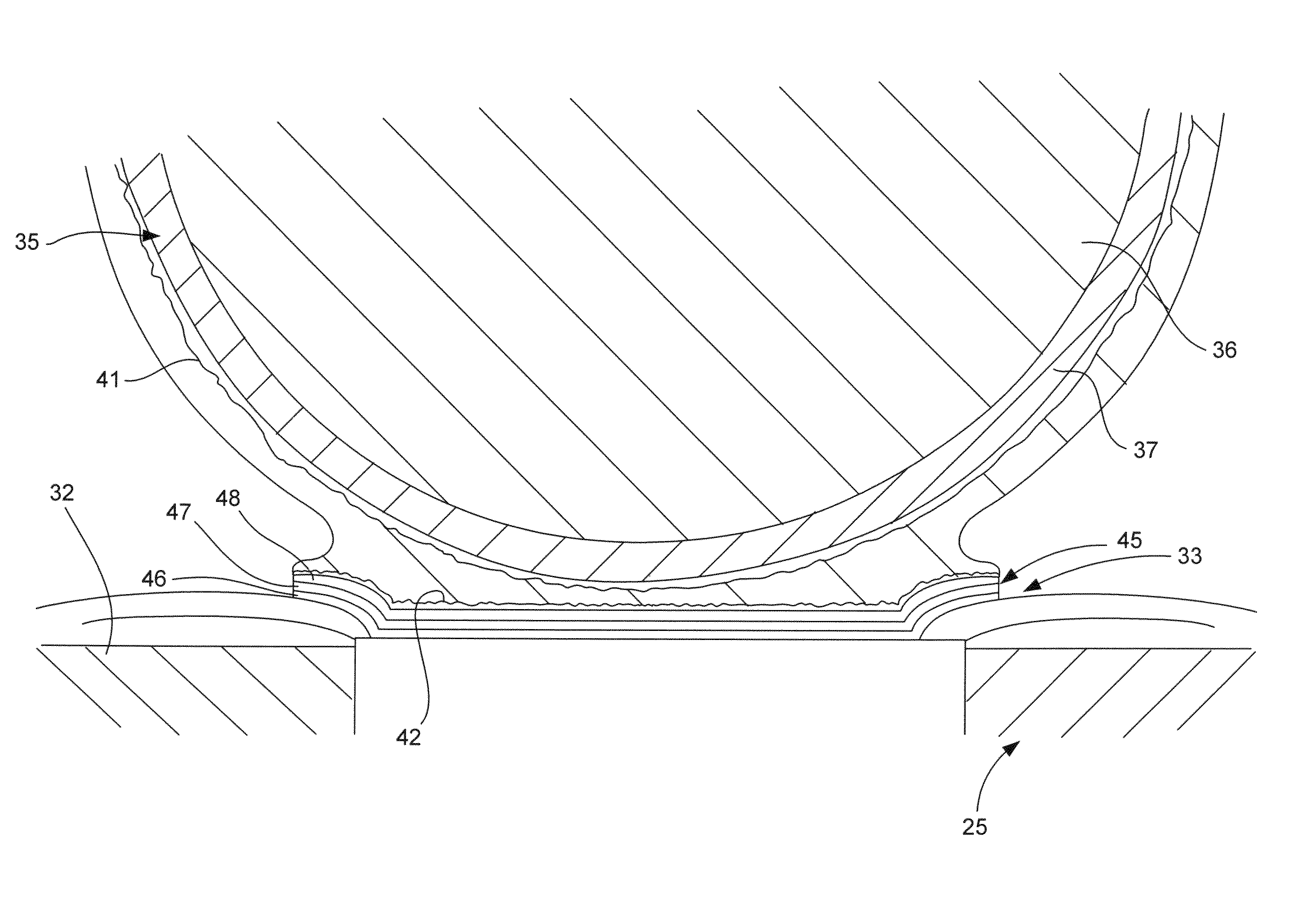
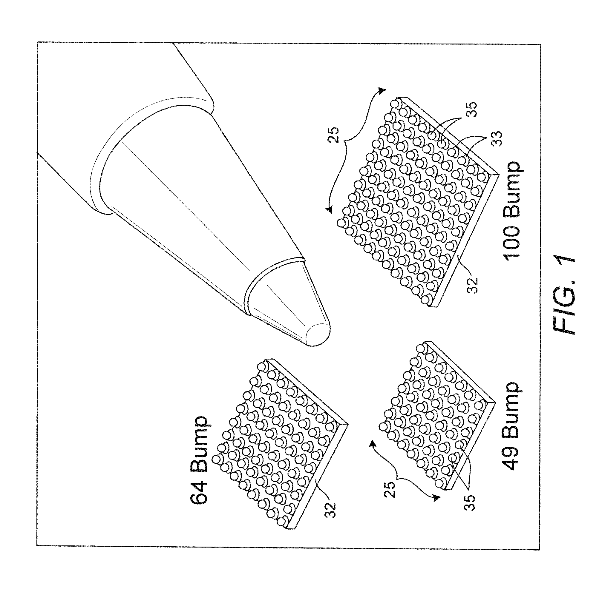
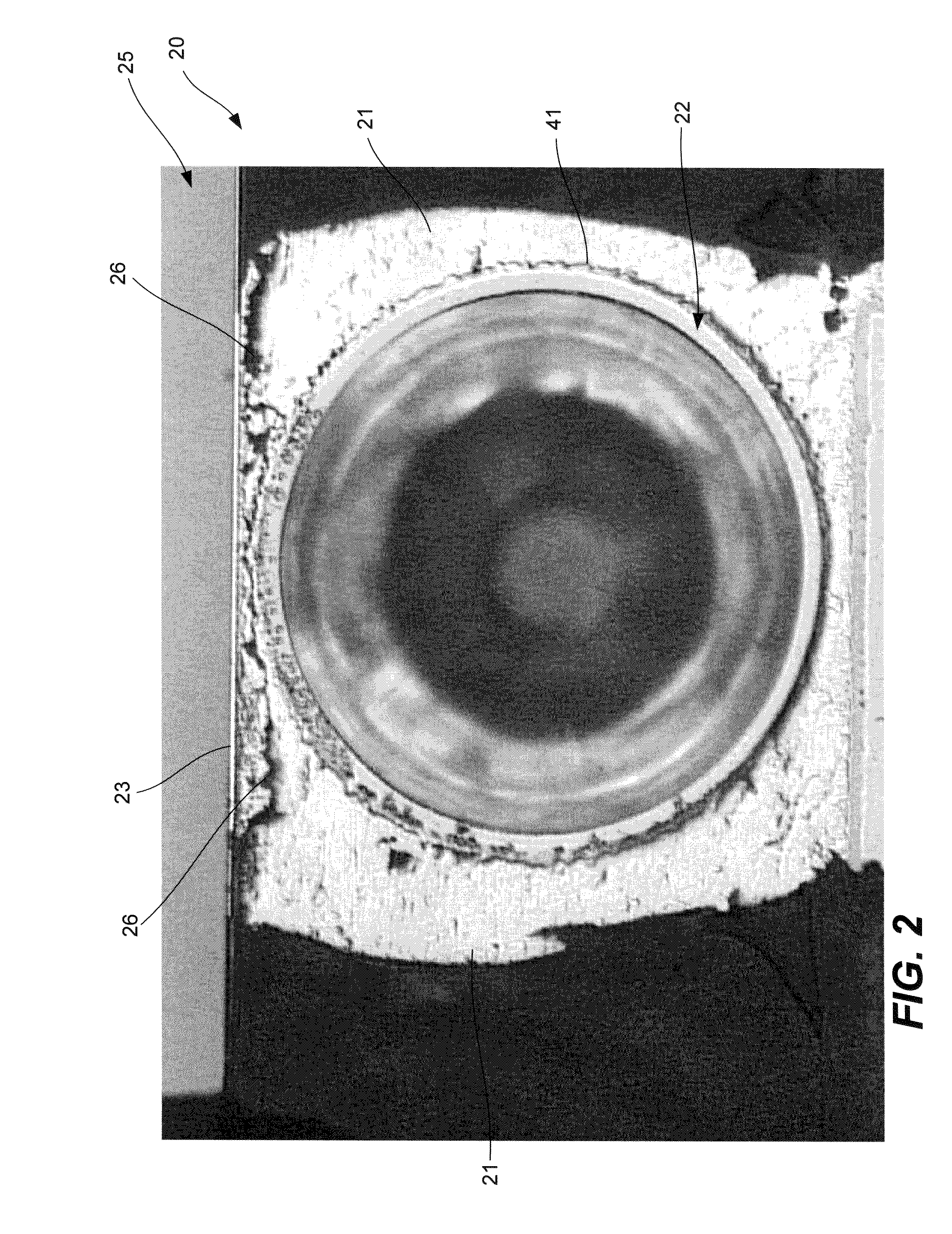
[0027]Referring now to the representative microelectronic package 25 of FIG. 1 and FIGS. 3-6, a high-strength solder joint, generally designated 30, is provided that is suitable for wafer level packages 25 and flip chip applications. More specifically, the present invention is particularly well suited for application with micro SMDxt package families beyond 100 bumps (e.g., 10×10 array outlines) that apply polymeric solder ball tec...


PUM

PropertyMeasurementUnit
Temperatureaaaaaaaaaa
Timeaaaaaaaaaa

Abstract

A Micro SMDxt package is provided that configured for mounting to a circuit board. The SMDxt package includes a silicon-based IC having an array of contact pads on one side of thereof, and a die electrically attached to the silicon-based IC. A plurality of solder balls is included, each of which has a polymeric core surrounded by a metallic shell that in turn is surrounded by a layer of solder material. Further, each solder ball is positioned in contact with a corresponding contact pad of the package. An intertwined intermetallic fusion layer is formed through the fusion between material components of the contact pads and the solder material, via heat treatment. The intermetallic fusion extends between and from an outer surface of the metallic shell of each solder to an outer surface of a corresponding contact pad to form a high strength intermetallic solder joint therebetween.

Description

BACKGROUND[0001]The present invention relates generally to the wafer level packaging, and more particularly relates to the formation of high strength solder joints thereon.[0002]There are a number of conventional arrangements for packaging integrated circuits. Many packaging techniques use a leadframe that has been stamped or etched from a metal (typically copper) sheet to provide electrical interconnects to external devices. One relatively recently developed packaging style, which is sometimes referred to as a Micro SMD (Surface Mount Devices) package, as shown in FIG. 1, which is wafer level CSP. In a micro SMD package, the footprint of the package is generally equal to that of the die size, yielding a relatively dense array outline of contacts on the active side of the silicon IC. In fact, these packages have one of the smallest footprints per I / O count.[0003]Typical micro SMD packages contain bump counts ranging from a four (4) (2×2 array outline) bump count to a thirty (30) bum...

Claims


Application Information

Patent Timeline
IPC IPC(8): H01L23/488B23K31/02H01L21/60
CPCB23K1/0016H01L2924/014H01L24/11H01L2224/13099H01L2224/16H01L2924/01013H01L2924/01022H01L2924/01029H01L2924/01047H01L2924/01082H01L2924/01327H01L2924/14H05K3/3436H05K2201/0212H05K2201/0221H01L2924/01006H01L2924/01033B23K2201/40H01L2224/13561H01L2224/13575H01L24/13B23K2101/40Y02P70/50
Inventor PATWARDHAN, VIRAJNGUYEN, HAU
Owner NAT SEMICON CORP
Why Eureka
Try Eureka