Magnetic sensor, hall element, hall ic, magnetoresistive effect element, method of fabricating hall element, and method of fabricating magnetoresistive effect element

a technology of magnetoresistive effect and hall element, applied in the field of magnetism, can solve the problem that the magnetism sensor cannot be used at a high temperature, and achieve the effect of the same measurement sensitivity

Inactive Publication Date: 2009-03-05
NGK INSULATORS LTD
View PDF3 Cites 19 Cited by
  • Summary
  • Abstract
  • Description
  • Claims
  • Application Information

AI Technical Summary

Benefits of technology

[0017]Accordingly, an object of the present invention is to provide a magnetic sensor which is operated better than that of the conventional magnetic sensor in the high temperature range not lower than 300° C.

Problems solved by technology

As described in Japanese Patent Application Laid-Open No. 2003-060255, in the case of the magnetic sensor for which InSb or InAs is used, there is widely known a drawback that the magnetic sensor cannot be used at a high temperature because of temperature dependence of a Hall voltage measured under a condition of constant magnetic flux density.

Method used


Image

  • Magnetic sensor, hall element, hall ic, magnetoresistive effect element, method of fabricating hall element, and method of fabricating magnetoresistive effect element
  • Magnetic sensor, hall element, hall ic, magnetoresistive effect element, method of fabricating hall element, and method of fabricating magnetoresistive effect element
  • Magnetic sensor, hall element, hall ic, magnetoresistive effect element, method of fabricating hall element, and method of fabricating magnetoresistive effect element

Examples


first embodiment

[0030]A Hall element which is of a magnetic sensor being able to detect a magnetic field by utilizing a semiconductor Hall effect will be described in a first embodiment.

(Outline of Hall Element)

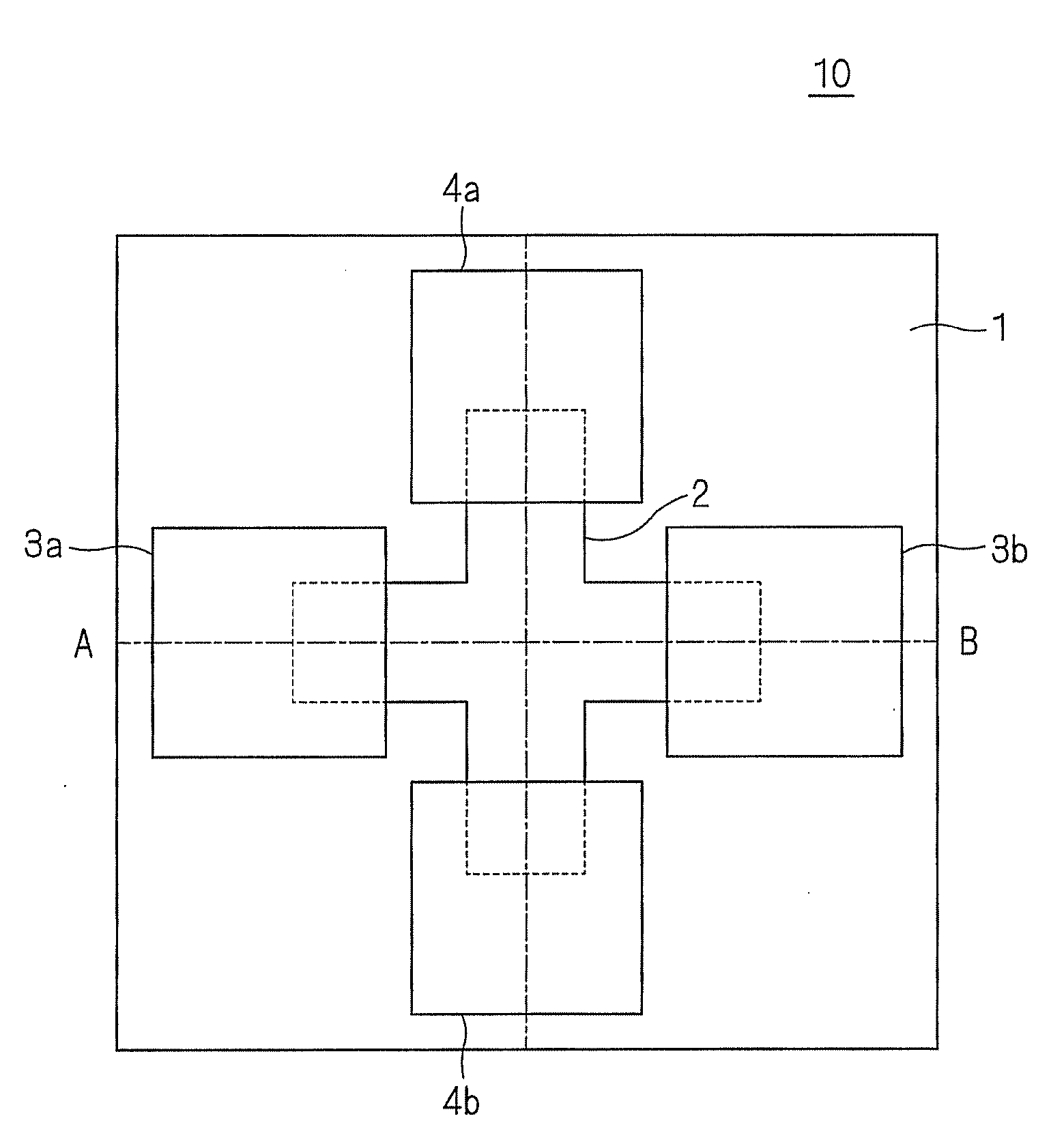
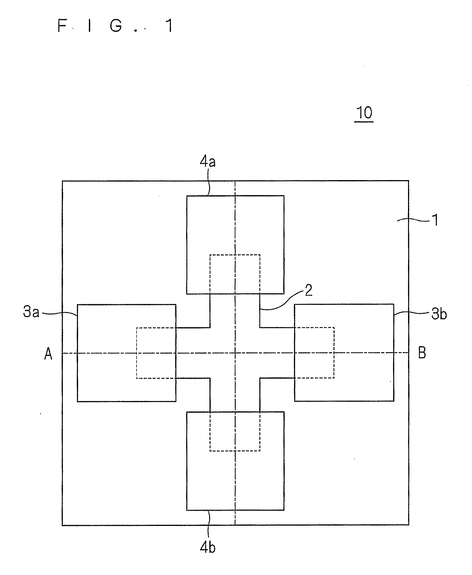
[0031]FIG. 1 is a top view showing a Hall element 10 according to the first embodiment of the present invention. FIG. 2 is a sectional view showing the Hall element 10 in a section A-B (passing through a substantially central portion) of FIG. 1.

[0032]In the Hall element 10, an operating layer 2, two input electrodes 3a and 3b, and two output electrodes 4a and 4b are provided on a substrate 1. The operating layer 2 is formed so as to have a cross shape in a central portion thereof when the Hall element 10 is viewed from above. Preferably each line of the cross shape is formed with a width of tens micrometers and a length of hundreds micrometers. For example, the width is set at 50 μm and the length is set at 200 μm.

[0033]The two input electrodes 3a and 3b are provided on front-end portions op...

second embodiment

(Outline of Hall Element)

[0062]As for the Hall element 10 shown in FIG. 2 of the first embodiment, when the operating layer 2 is formed into the cross shape with the RIE technique, a part of the substrate 1 is also removed by performing the etching deeper than the thickness of the operating layer 2. The way of forming the operating layer 2 into the cross shape is not limited to such manner. A Hall element including an operating layer in a different manner from the Hall element according to the first embodiment will be described in this embodiment.

[0063]FIG. 13 is a sectional view showing a section passing through a substantially central portion of a Hall element 20 according to the second embodiment. The Hall element 20 according to the second embodiment differs from the Hall element 10 according to the first embodiment in that the height of the cross-shape portion of the Hall element 20 is lower than that of the Hall element 10, although the Hall element 20 is identical to the Hall...

third embodiment

[0073]The laminated structure 5 prepared for the fabrication of the Hall element 20 according to the second embodiment, which has the first layer 2a made of the high-resistance GaN layer whose specific resistance is not lower than 1×10⁶ Ωcm (electron concentration is not more than 1×10¹² / cm3), suitably satisfies conditions to fabricate a high electron mobility transistor (HEMT) exhibiting a good pinch-off characteristic. Accordingly, by utilizing the laminated structure 5, a Hall IC in which the Hall element according to the second embodiment and an IC unit including HEMT are integrated can be realized. The Hall IC will be described in a third embodiment.

[0074]FIG. 14 is a side view showing a conceptual configuration of a Hall IC 100 according to the third embodiment. FIG. 15 is a top view showing a conceptual configuration of the Hall IC 100 according to the third embodiment. In the Hall IC 100 shown in FIGS. 14 and 15, the components are disposed by way of example for the purpose ...


PUM


Abstract

An aspect of the present invention provides a magnetic sensor which is operated better at a high temperature range not lower than 300° C. compared with a conventional magnetic sensor. A operating layer having a heterojunction interface is formed by laminating a first layer made of GaN whose electron concentration is not more than 1×10¹⁶ / cm3 at room temperature and a second layer made of AlxGa1-xN (0<x≦0.3). Therefore, in a two-dimensional electron gas region, carrier mobility is further enhanced while a carrier concentration is further lowered. Accordingly, there is realized a Hall element which can be used with measurement sensitivity similar to that at room temperature by constant-current drive even at a high temperature, while having the high measurement sensitivity in both the constant-current drive and constant-voltage drive at room temperature.

Description

BACKGROUND OF THE INVENTION[0001]1. Field of the Invention[0002]The present invention relates to a magnetic sensor whose operating layer is made of a group-III nitride semiconductor.[0003]2. Description of the Background Art[0004]It is known that magnetic sensors such as a Hall element and a magnetoresistive effect element whose operating layer is made of a semiconductor material exhibit higher sensitivity with increasing carrier mobility of the semiconductor material used. Therefore, conventionally compound semiconductors such as InSb and InAs which exhibit high electron mobility have been used for the operating layer of the magnetic sensor (refer to, e.g., “Physical properties of InSb single-crystal thin film and magnetic sensor application”, IEEJ Transactions on Electrical and Electronic Engineering E, Vol. 123, No. 3 (2003), pp. 69-78). For example, the Hall element in which Hall effect of a thin-film of InSb or InAs is utilized is extensively used as a magnetic sensor of DC bru...

Claims


Application Information

Patent Timeline
Patent Type & Authority Applications(United States)
IPC IPC(8): G01R33/07
CPCG01R33/07
Inventor MIYOSHI, MAKOTOTANAKA, MITSUHIRO
Owner NGK INSULATORS LTD
Why Eureka
Try Eureka