Stack chip and stack chip package having the same

a technology of stack chip and stack chip, which is applied in the direction of solid-state devices, basic electric elements, lighting and heating apparatus, etc., can solve the problems of preventing high-speed operation of the semiconductor package and/or the system, reducing signal integrity, etc., to reduce the input capacitive load of the semiconductor package, improve the speed and capacity of the package, and reduce the number of standby input/output buffers

Active Publication Date: 2009-03-12
SAMSUNG ELECTRONICS CO LTD
View PDF8 Cites 16 Cited by
  • Summary
  • Abstract
  • Description
  • Claims
  • Application Information

AI Technical Summary

Benefits of technology

[0011]Embodiments of the invention reduce the input capacitive loading of a semiconductor package to improve the speed and capacity of the package. The embodiments also reduce the number of standby input / output buffers and prevent reduction of the valid window size of data at the system level to improve the signal integrity of the package.

Problems solved by technology

Therefore, reduction of signal integrity may prevent high speed operation of the semiconductor package and / or the system.

Method used


Image

  • Stack chip and stack chip package having the same
  • Stack chip and stack chip package having the same
  • Stack chip and stack chip package having the same

Examples


Embodiment Construction

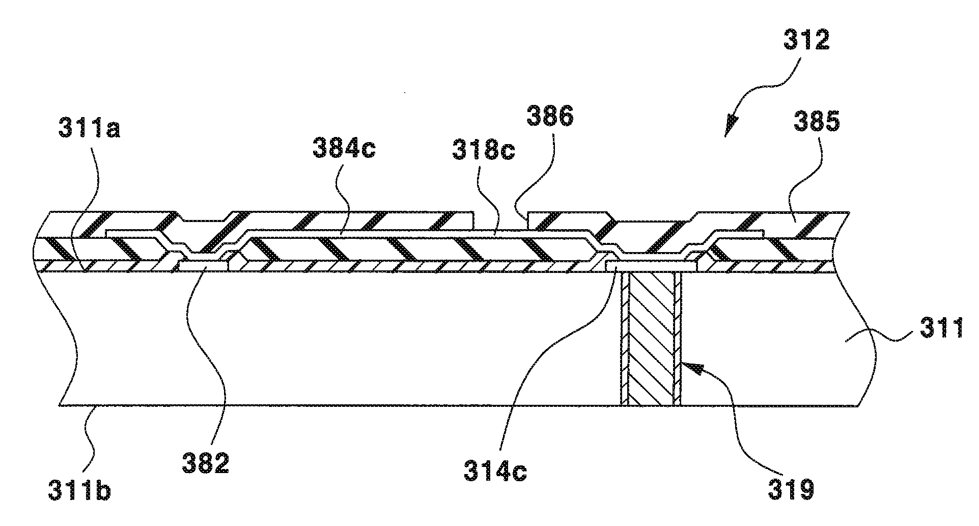
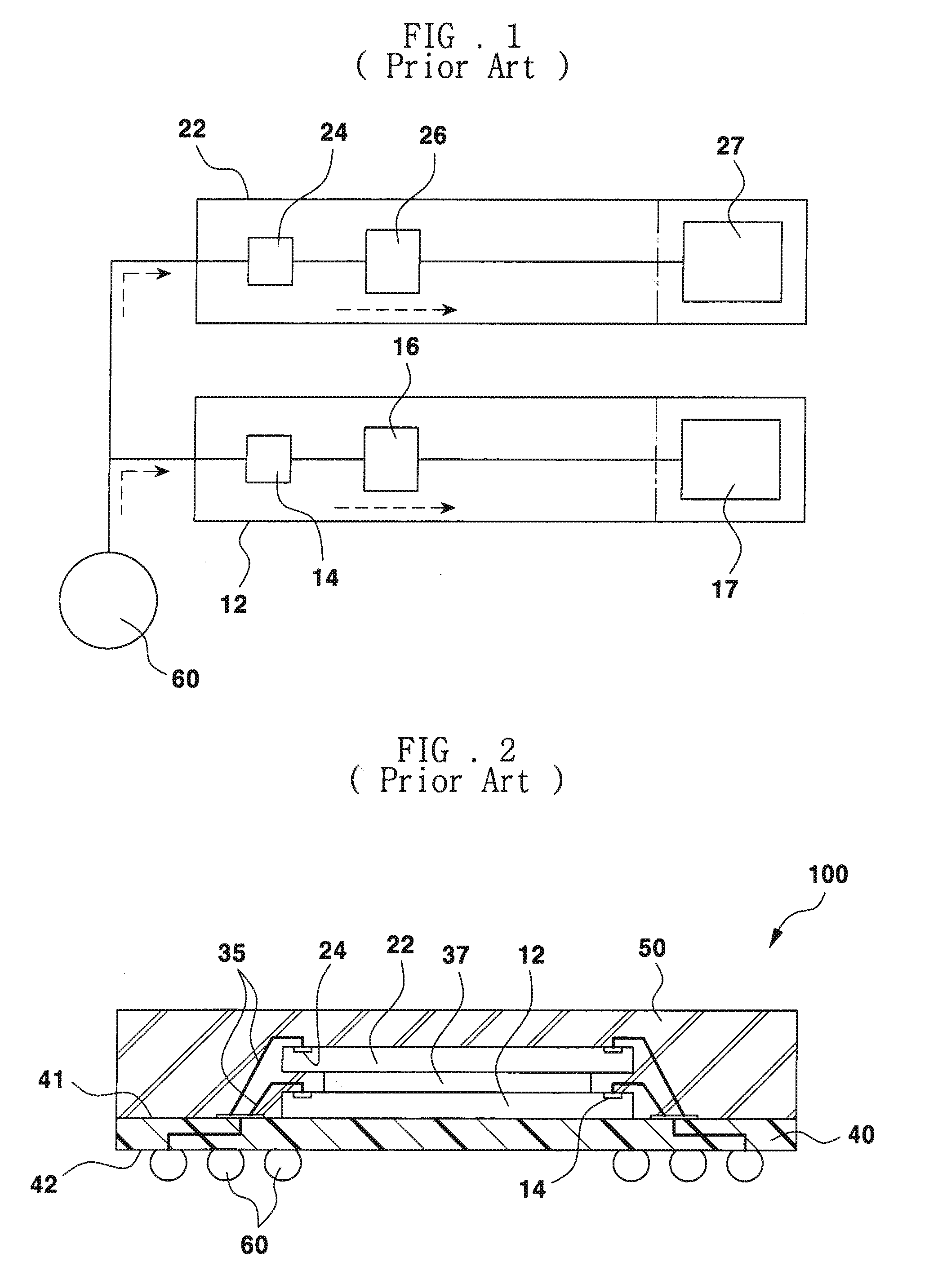
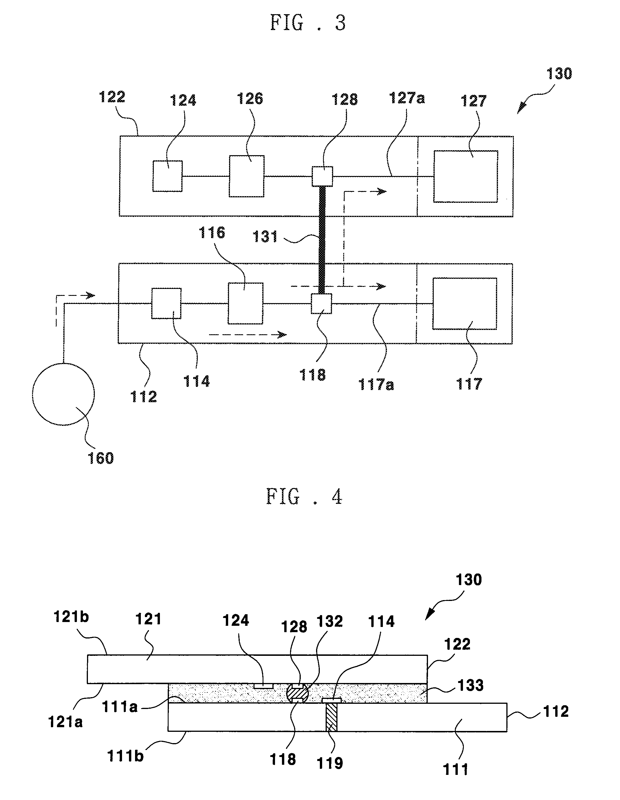
[0028]Example, non-limiting embodiments of the invention are described more fully hereinafter with reference to the accompanying drawings. This invention may, however, be embodied in many different forms and should not be construed as limited to the example embodiments set forth herein. Rather, the disclosed embodiments are provided so that this disclosure will be thorough and complete, and will fully convey the scope of the invention to those skilled in the art. The principles and features of this invention may be employed in varied and numerous embodiments without departing from the scope of the invention.

[0029]It should be noted that the figures are intended to illustrate the general characteristics of methods and devices of example embodiments of this invention, for the purpose of the description of such example embodiments herein. These drawings are not, however, to scale and may not precisely reflect the characteristics of any given embodiment, and should not be interpreted as...


PUM


Abstract

Provided are a stack chip and a stack chip package having the stack chip. Internal circuits of two semiconductor chips are electrically connected to each other through an input / output buffer connected to an external connection terminal. The semiconductor chip has chip pads, input / output buffers and internal circuits connected through circuit wirings. The semiconductor chip also has connection pads connected to the circuit wirings connecting the input / output buffers to the internal circuits. The semiconductor chips include a first chip and a second chip. The connection pads of the first chip are electrically connected to the connection pads of the second chip through electrical connection means. Input signals input through the external connection terminals are input to the internal circuits of the first chip or the second chip via the chip pads and the input / output buffers of the first chip, and the connection pads of the first chip and the second chip.

Description

CROSS-REFERENCE TO RELATED PATENT APPLICATION[0001]This application is a Continuation of U.S. patent application Ser. No. 11 / 627,791, filed on Jan. 26, 2007, now pending, which claims priority from Korean Patent Application No. 2006-8304 filed on Jan. 26, 2006, all of which are hereby incorporated by reference in their entirety.BACKGROUND[0002]1. Technical Field[0003]The invention relates to a semiconductor packaging technique and, more particularly, to a stack chip and a semiconductor package having the stack chip.[0004]2. Description of the Related Art[0005]Memory product development, for example DRAM development, has been focused on moving towards increased speed and capacity. One method for improving capacity is a chip stacking technique that may be used to stack semiconductor chips on a limited area of a package. The chip stacking may increase capacity of a product corresponding to the number of the semiconductor chips used.[0006]In semiconductor packages manufactured by chip s...

Claims


Application Information

Patent Timeline
Patent Type & Authority Applications(United States)
IPC IPC(8): H01L23/52
CPCH01L23/13H01L2224/73257H01L24/73H01L25/0657H01L2224/48091H01L2224/48227H01L2224/4824H01L2225/0651H01L2225/06527H01L2225/06562H01L2924/01013H01L2924/01029H01L2924/01057H01L2924/01079H01L2924/01082H01L2924/15311H01L23/66H01L2924/01033H01L24/48H01L2924/01006H01L2924/00014H01L2924/14H01L2924/00H01L2224/45099H01L2224/45015H01L2924/207B60Q3/88F21V23/004B60Y2200/11
Inventor LEE, JONG-JOOLEE, DONG-HO
Owner SAMSUNG ELECTRONICS CO LTD
Why Eureka
Try Eureka