Piezoelectric device, liquid droplet ejecting head using the same, and process for producing the same

a technology of liquid droplet ejection and piezoelectric film, which is applied in the direction of piezoelectric/electrostrictive transducers, device material selection, generators/motors, etc., can solve the problems of high probability of pyrochlore phase formation, inability to enhance inability to enhance device reproducibility, so as to achieve enhanced piezoelectric characteristics and durability, the effect of preventing pb loss

Inactive Publication Date: 2009-03-12
FUJIFILM CORP
View PDF3 Cites 11 Cited by
  • Summary
  • Abstract
  • Description
  • Claims
  • Application Information

AI Technical Summary

Benefits of technology

[0009]It is therefore an object of the present invention to solve the aforementioned problems of the prior art and provide a piezoelectric device having high piezoelectric characteristics and durability.
[0039]According to the third aspect of the present invention, the amount of Pb that contributes to the early stage of growth by a vapor phase deposition can be increased to thereby prevent the occurrence of Pb loss, as well as preventing or at least controlling the formation of a pyrochlore phase. This enables the production of a piezoelectric device that has a particularly small content of the pyrochlore phase near the interface, and as a result, piezoelectric devices having high piezoelectric characteristics and durability can be manufactured with high reproducibility.

Problems solved by technology

However, both methods involve an annealing treatment, so not only is unstable the lead concentration in the surface area of the piezoelectric film (the region closer to the upper electrode) but it is also impossible to enhance the piezoelectric characteristics and durability.
Aside from this problem, the additional process makes it impossible to enhance the reproducibility of the device.
A problem with the production of a piezoelectric film by a vapor phase deposition such as a sputtering method is high likelihood for the formation of a pyrochlore phase.
A piezoelectric film rich in the pyrochlore phase has such low piezoelectric characteristics and durability that its performance as a piezoelectric device is low.
Consequently, piezoelectric devices that use a piezoelectric film prepared by a sputtering method suffer scattering in performance and, hence, are low in reproducibility.

Method used


Image

  • Piezoelectric device, liquid droplet ejecting head using the same, and process for producing the same
  • Piezoelectric device, liquid droplet ejecting head using the same, and process for producing the same
  • Piezoelectric device, liquid droplet ejecting head using the same, and process for producing the same

Examples


example 1

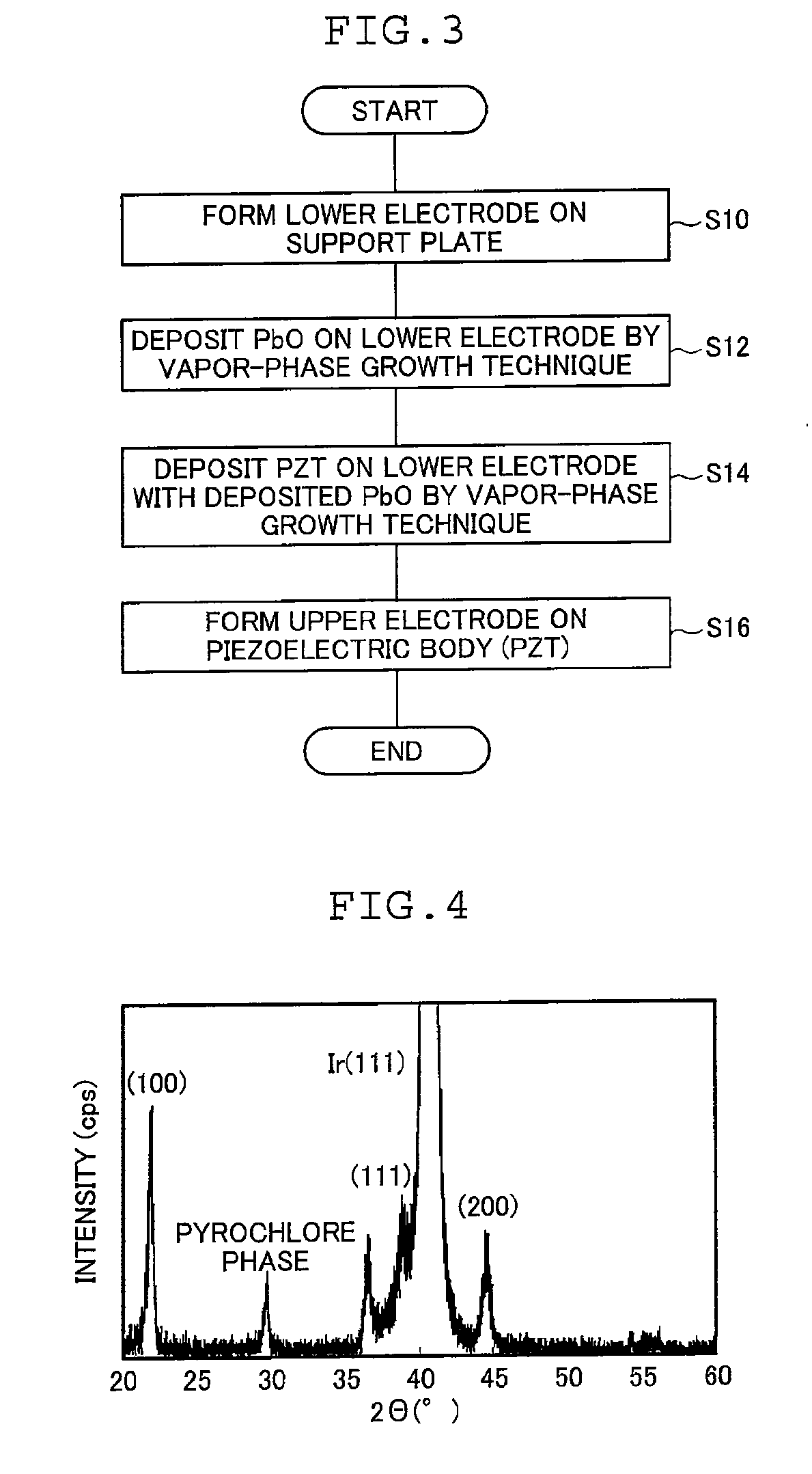
[0125]The piezoelectric device used in Example 1 was fabricated by the following procedure.

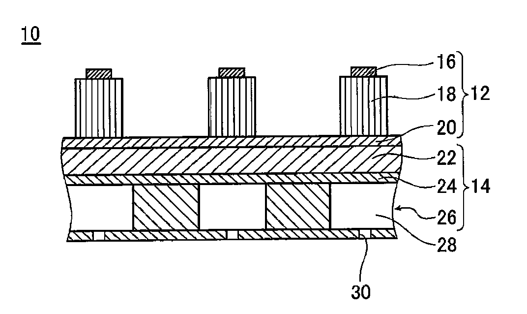
[0126]An SOI substrate was used as the support. The lower electrode was formed on the SOI substrate by sputtering. More specifically, with the SOI substrate heated at 350° C., Ti was evaporated to a thickness of 10 nm on the SOI substrate and Ir was then evaporated to a thickness of 300 nm to fabricate the lower electrode.

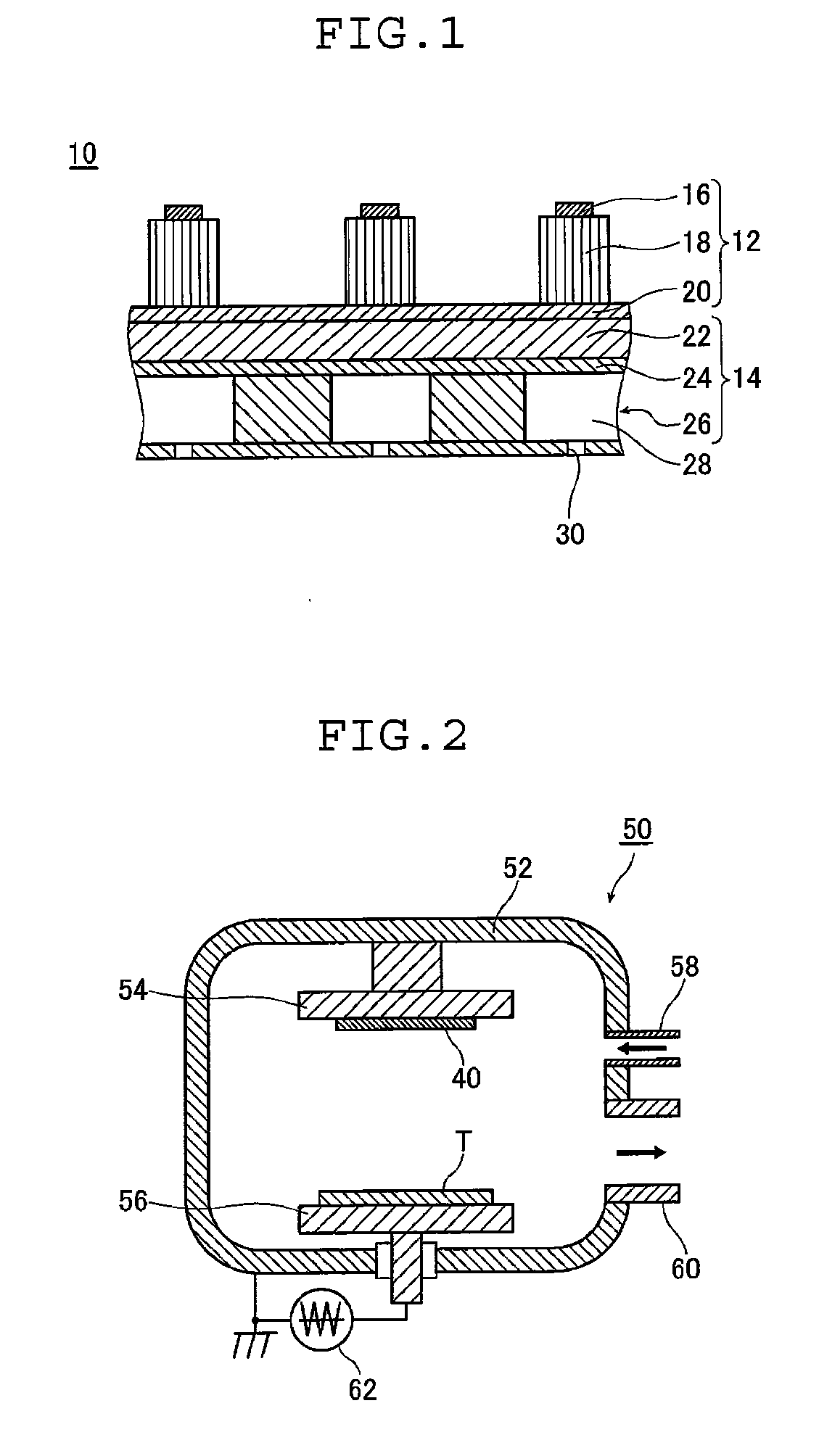
[0127]Subsequently, the SOI substrate with the lower electrode was set up within the sputtering apparatus 50 and a PbO sinter was also set up as the target. Thereafter, as it was degassed, the vacuum vessel was supplied with Ar gas to establish an Ar atmosphere having a total pressure of 0.3 Pa; the SOI substrate was further heated to 450° C. Under these conditions, sputtering was performed to deposit PbO to a thickness of 10 nm on the lower electrode.

[0128]Then, the target was changed to Pb1.3((Zr0.52Ti0.48)0.9Nb0.10)O3 and a gaseous mixture of Ar / 1% O2 (consisting of Ar and...

examples 2 to 5

[0138]The film deposition conditions of Example 1 were changed in such a way that Pb mass / (Zr+Ti+Nb) mass at the site of 100 nm thickness would be 0.8 (Example 2), 1.0 (Example 3), 1.4 (Example 4) and 1.6 (Example 5). The thus fabricated piezoelectric devices were subjected to the same measurements and calculations as in Example 1.

[0139]The results of the measurements and calculations were as follows. In Example 2, the piezoelectric constant d31 was 240 pm / V, the ratio of perovskite peaks to pyrochlore peaks at 100 nm thickness was 0.2, and point A / point B was 0.7.

[0140]In Example 3, the piezoelectric constant d31 was 250 pm / V, the ratio of perovskite peaks to pyrochlore peaks at 100 nm thickness was 0.1, and point A / point B was 0.9.

[0141]In Example 4, the piezoelectric constant d31 was 250 pm / V, the ratio of perovskite peaks to pyrochlore peaks at 100 nm thickness was 8.2, and point A / point B was 1.3.

[0142]In Example 5, the piezoelectric constant d31 was 240 pm / V, the ratio of pero...


PUM

PropertyMeasurementUnit
thicknessaaaaaaaaaa
thicknessaaaaaaaaaa
dielectric constantaaaaaaaaaa

Abstract

The piezoelectric device includes a piezoelectric film that expands or contracts according to variations in voltage applied, a first electrode provided on a first side of the film, and a second electrode provided on a second side of the film. The film is formed on the second electrode by a vapor phase deposition and mainly composed of PbxByOz. An element at site B is at least one element selected from the group consisting of Ti, Zr, V, Nb, Ta, Cr, Mo, W, Mn, Sc, Co, Cu, In, Sn, Ga, Zn, Cd, Fe, and Ni, and 0<x≦1, 0<y≦1, and 2.5<z≦3. A first value of x / y in a first area of the film 100 nm apart from a surface of contact with the second electrode toward the first electrode ranges from 0.8 to 1.6 or is 0.7 times or more but not greater than 1.5 times a second value of x / y in a center area of the film, or the first area has a ratio of perovskite peaks to pyrochlore peaks as measured by XRD of 0.2 or more.

Description

[0001]The entire contents of documents cited in this specification are incorporated herein by reference.BACKGROUND OF THE INVENTION[0002]The present invention relates to a piezoelectric device, a liquid droplet ejecting head using the same, and a process for producing the same.[0003]Conventionally known actuator is a piezoelectric device in which a piezoelectric film having such a piezoelectric effect that it is displaced in response to voltage application is combined with electrodes that apply voltage to the piezoelectric film. Examples of this piezoelectric device are described in JP 2005-101512 A, JP 5-235268 A, and JP 2000-299510 A and their piezoelectric films use a lead oxide such as lead zirconate titanate (also known as PZT).[0004]JP 2005-101512 A describes a piezoelectric device comprising a piezoelectric film that consists of PZT to which niobium (Nb) has been added. By adding niobium, PbO loss is prevented and the occurrence of an unwanted phase near the interface between...

Claims


Application Information

Patent Timeline
Patent Type & Authority Applications(United States)
IPC IPC(8): H02N2/04B41J2/045H01L41/22B41J2/055B41J2/135B41J2/14B41J2/16C23C14/08H01L41/09H01L41/18H01L41/316H01L41/319H02N2/00
CPCB41J2/14233B41J2/161B41J2/1646Y10T29/42H01L41/316H01L41/0973H01L41/1876H10N30/1051H10N30/2047H10N30/8554H10N30/076
Inventor NAONO, TAKAYUKIARAKAWA, TAKAMIFUJII, TAKAMICHI
Owner FUJIFILM CORP
Why Eureka
Try Eureka