Gate drive circuit

a drive circuit and gate technology, applied in logic circuit coupling/interface arrangement, pulse generator, pulse technique, etc., can solve the problems of device degradation, device transition to an off state, device voltage further decrease, etc., to prevent an increase in steady state loss, the switching characteristics of the power semiconductor device can be arbitrarily set, and the resistance to short circuiting is sufficient.

Active Publication Date: 2009-03-12
MITSUBISHI ELECTRIC CORP
View PDF2 Cites 89 Cited by
  • Summary
  • Abstract
  • Description
  • Claims
  • Application Information

AI Technical Summary

Benefits of technology

[0008]The present invention has been devised to solve the above problems. It is, therefore, an object of the present invention to provide a gate drive circuit which can drive a power semiconductor device in such a way that the device exhibits sufficient resistance to short circuiting while preventing an increase in its steady state loss, and which enables the switching characteristics of the power semiconductor device to be arbitrarily set.

Problems solved by technology

Then, after a delay caused by another delay circuit, the same turn-off voltage is directly applied to the gate of the power semiconductor device, so that the gate voltage further decreases, with the result that the device transitions to an off state.
However, this gate drive circuit is disadvantageous in that if the arm in which the power semiconductor device is connected suffers a short circuit, a large current flows through the device since its gate voltage is relatively high, which may lead to degradation of the device.
However, this results in an increase in the steady state loss in the device.
Thus, with the gate drive circuit of the above patent publication, a power semiconductor device cannot exhibit sufficient resistance to short circuiting.

Method used


Image

  • Gate drive circuit
  • Gate drive circuit
  • Gate drive circuit

Examples


first embodiment

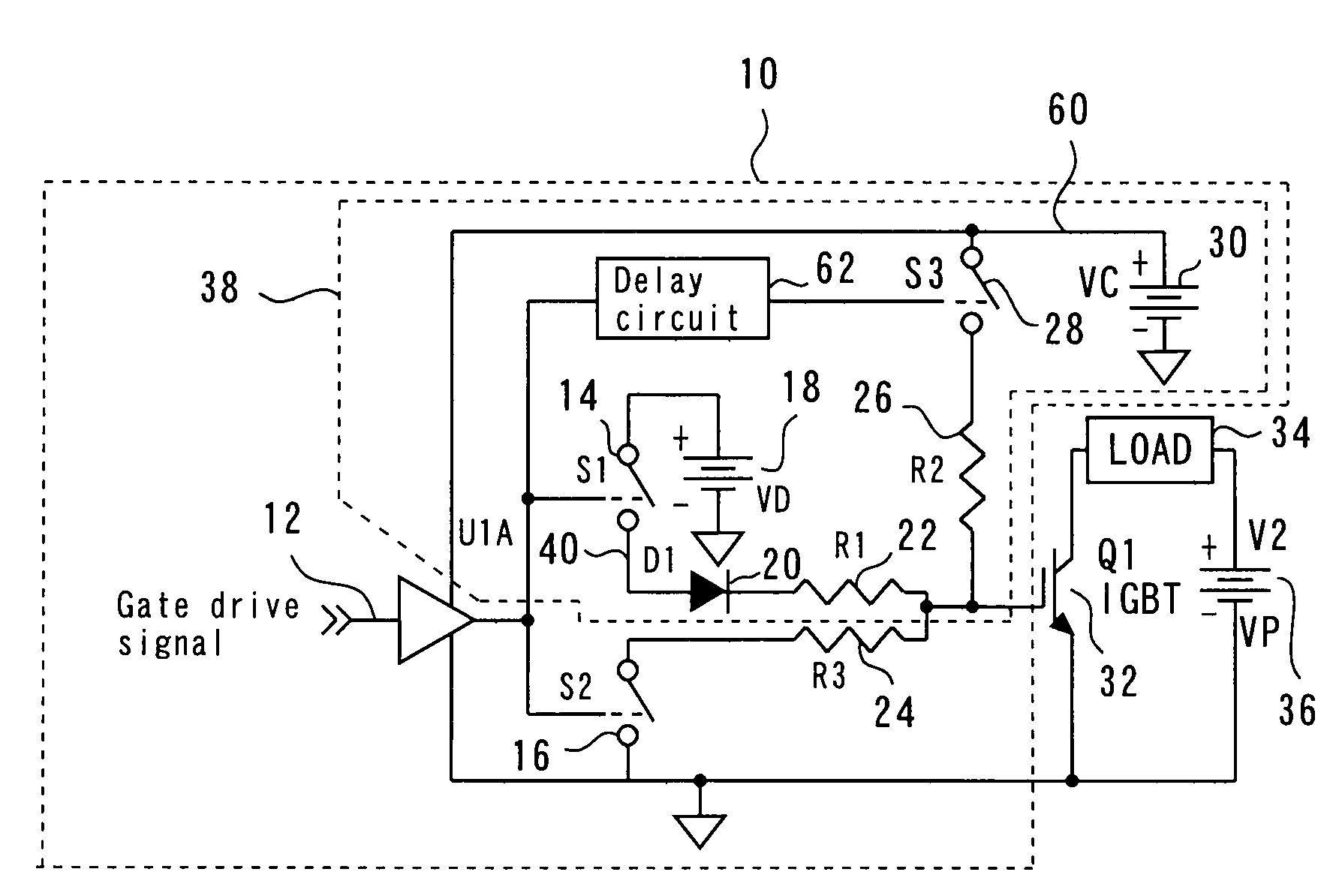
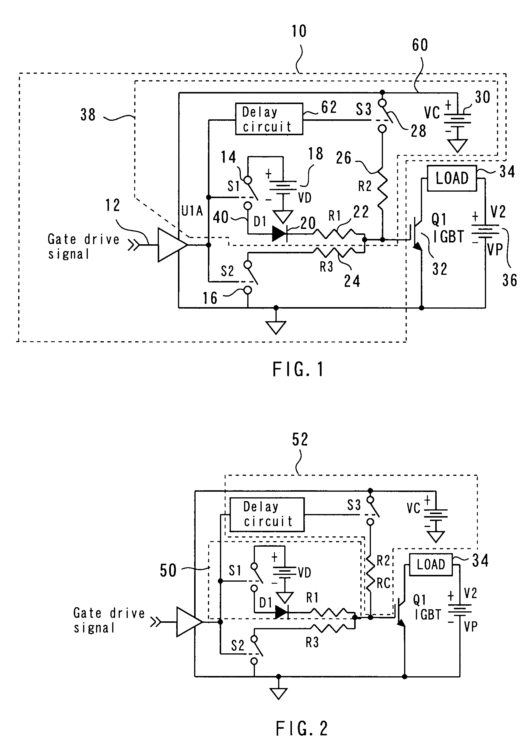
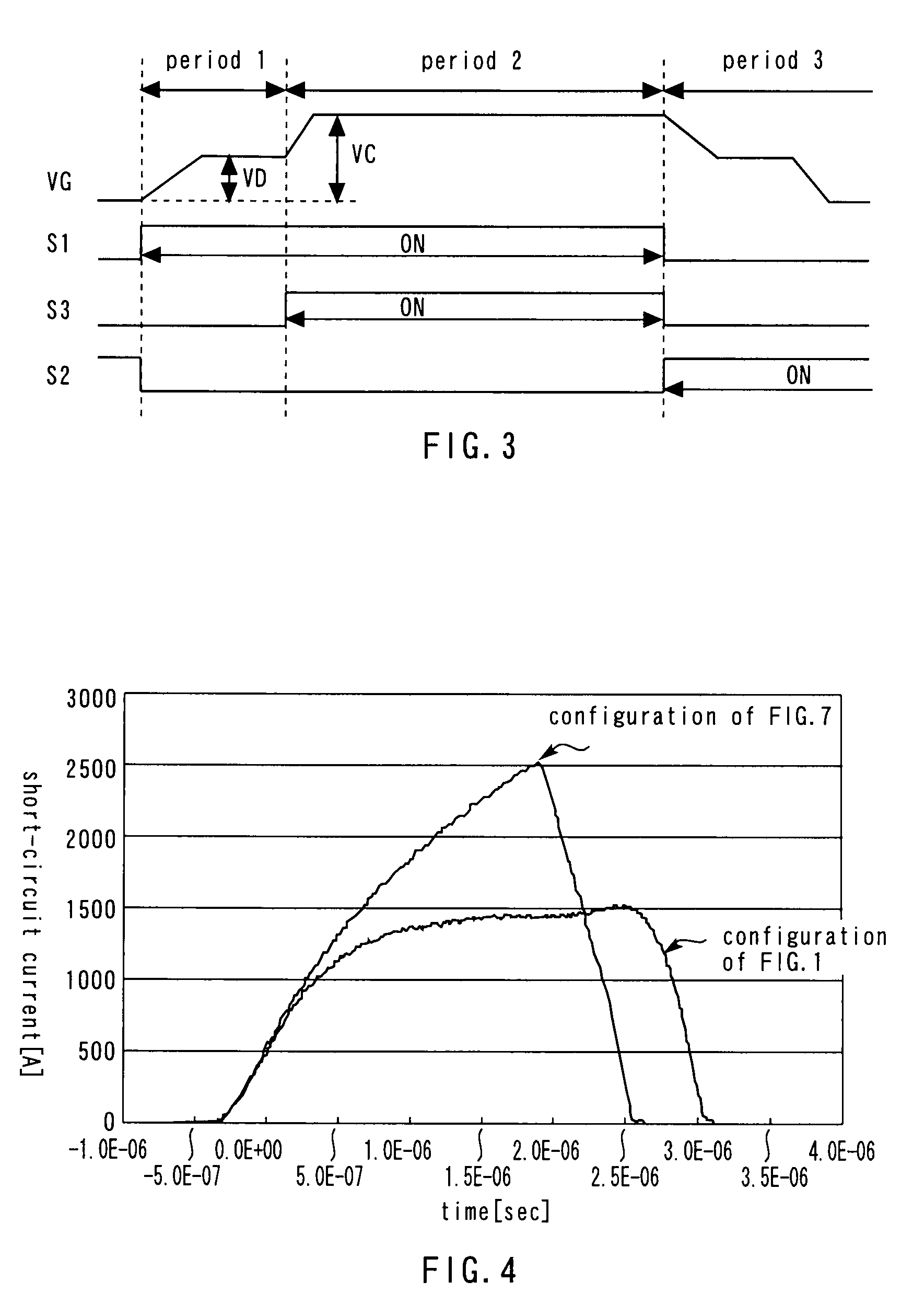
[0069]A first embodiment of the present invention provides a gate drive circuit that can drive a power switching device in such a way as to optimize its turn-on characteristics. FIG. 1 is a circuit diagram illustrating the configuration of this gate drive circuit (10). In FIG. 1, the gate drive circuit 10 drives the gate of a power switching device 32. The power switching device 32 may be a voltage driven bipolar transistor, a MOSFET, etc. The following description of the present embodiment assumes that the device 32 is an IGBT (Insulated Gate Bipolar Transistor) and constitutes a portion of an arm (a bridge or shunt arm).

[0070]The gate drive circuit 10 includes a turn-on side circuit 38 for turning on the power switching device 32. The turn-on side circuit 38 includes a first turn-on side power supply circuit 50 and a second turn-on side power supply circuit 52, as shown in FIG. 2. First the first turn-on side power supply circuit 50 will be described with reference to FIG. 1. The ...

second embodiment

[0102]A second embodiment of the present invention provides a gate drive circuit that can drive a power switching device in such way as to optimize its turn-off switching characteristics. FIG. 11 is a diagram illustrating the configuration of this gate drive circuit (100). Referring to FIG. 11, the gate drive circuit 100 includes a turn-off side circuit 102 for turning off a power switching circuit 32. Further, the gate drive circuit 100 also includes a turn-on side circuit (which does not overlap the turn-off side circuit 102) for turning on the power switching circuit 32. It should be noted that the power switching device 32 is set to a steady on state by turning on a turn-on side switch 132 in the turn-on side circuit and thereby applying a voltage VC to the gate of the power switching device 32.

[0103]FIG. 12 is a diagram illustrating the turn-off side circuit 102 described with reference to FIG. 11. The turn-off side circuit 102 includes a first turn-off side power supply circui...

third embodiment

[0118]A third embodiment of the present invention provides a gate drive circuit that includes a simple, low cost circuit for changing the first turn-on voltage. This gate drive circuit differs from that shown in FIG. 1 in that the first turn-on voltage 18 is replaced by the turn-on side variable voltage circuit 300 shown in FIG. 16. That is, according to the present embodiment, the first turn-on voltage is supplied from this turn-on side variable voltage circuit 300 instead of the first turn-on voltage source 18. The output terminal OUTPUT of the turn-on side variable voltage circuit 300 is connected to the first turn-on wiring 40. The turn-on side variable voltage circuit 300 supplies the first turn-on voltage (also denoted by Vout herein), as described above. It should be noted that the configuration and operation of the gate drive circuit of the present embodiment are similar to those of the gate drive circuit of the first embodiment except that the first turn-on voltage is suppl...


PUM


Abstract

A gate drive circuit includes a turn-on side circuit for turning on a gate of a power switching device, the turn-on side circuit including a first turn-on side power supply circuit and a second turn-on side power supply circuit, the first turn-on side power supply circuit including: a first turn-on voltage source for supplying a first turn-on voltage; first turn-on wiring; and a first turn-on switch connected in the first turn-on wiring and controlled by a gate drive signal; and the second turn-on side power supply circuit including: a second turn-on voltage source for supplying a second turn-on voltage applied to the gate of the power switching device to set the power switching device in a steady (on) state; second turn-on wiring; a second turn-on switch connected in the second turn-on wiring; and a turn-on side delay circuit for delaying the gate drive signal and passing it to the second turn-on switch.

Description

BACKGROUND OF THE INVENTION[0001]1. Field of the Invention[0002]The present invention relates to gate drive circuits adapted to improve the switching characteristics of devices and more particularly adapted to improve the switching characteristics of power switching devices.[0003]2. Background Art[0004]A bridge circuit such as an inverter generally includes a plurality of power semiconductor devices. Examples of power semiconductor devices which are widely used in bridge circuits include voltage driven power semiconductor devices such as IGBTs (Insulated Gate Bipolar Transistors) and MOSFETs. A circuit for controlling the gate voltage of a voltage driven power semiconductor device is commonly referred to as a “gate drive circuit.” That is, a gate drive circuit is used to cause a power semiconductor device to perform a switching operation.[0005]JP-A-2001-37207 discloses an exemplary gate drive circuit for driving a power semiconductor device, which includes a turn-on side circuit for...

Claims


Application Information

Patent Timeline
Patent Type & Authority Applications(United States)
IPC IPC(8): H03K17/28
CPCH03K17/08128H03K17/163H03K17/168H03K2217/0036H03K17/567H03K17/74H03K17/284
Inventor HIYAMA, KAZUAKI
Owner MITSUBISHI ELECTRIC CORP
Why Eureka
Try Eureka