Programming method of flash memory device

Active Publication Date: 2009-03-12
SK HYNIX INC
View PDF7 Cites 9 Cited by
  • Summary
  • Abstract
  • Description
  • Claims
  • Application Information

AI Technical Summary

Benefits of technology

[0029]According to the present invention, although the sequence of the LSB programming operation and the MSB programming operation and the sequence of word lines that are programmed are changed, a programming operation (in particular, the MSB programming operation) can be performed in a state where the channel region is precharged to the same level within a string. Accordingly, a phenomenon can be prevented in which a channel region of third memory cells located between a source select transistor and a first memory cell on which the programming operation is performed within the same string is precharged to a low voltage level. Consequently, the voltage difference between a word line and a channel region of the third memory cells can be maintained at a low level. Accordingly, the third memory cell can be prevented from being programmed when a programming operation of the third memory cell should not be performed.

Problems solved by technology

However, during the programming operation, the threshold voltage of a memory cell connected to a word line adjacent to the selected word line can be changed due to an interference phenomenon between memory cells.

Method used


Image

  • Programming method of flash memory device
  • Programming method of flash memory device
  • Programming method of flash memory device

Examples


Embodiment Construction

[0034]Embodiments according to the present invention will be described with reference to the accompanying drawings.

[0035]The present invention is not limited to the disclosed embodiments, but may be implemented in various manners. The embodiments are provided to complete the disclosure of the present invention and to allow those having ordinary skill in the art to understand the scope of the present invention. The present invention is defined by the scope of the claims.

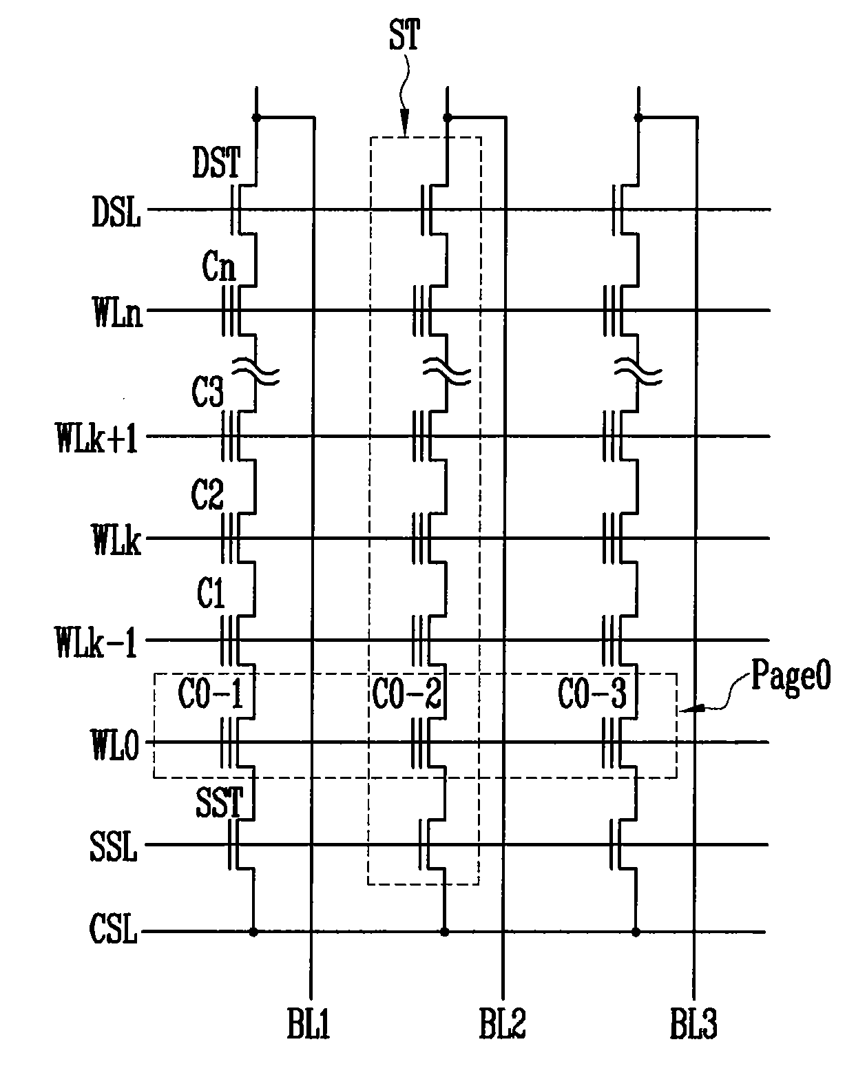
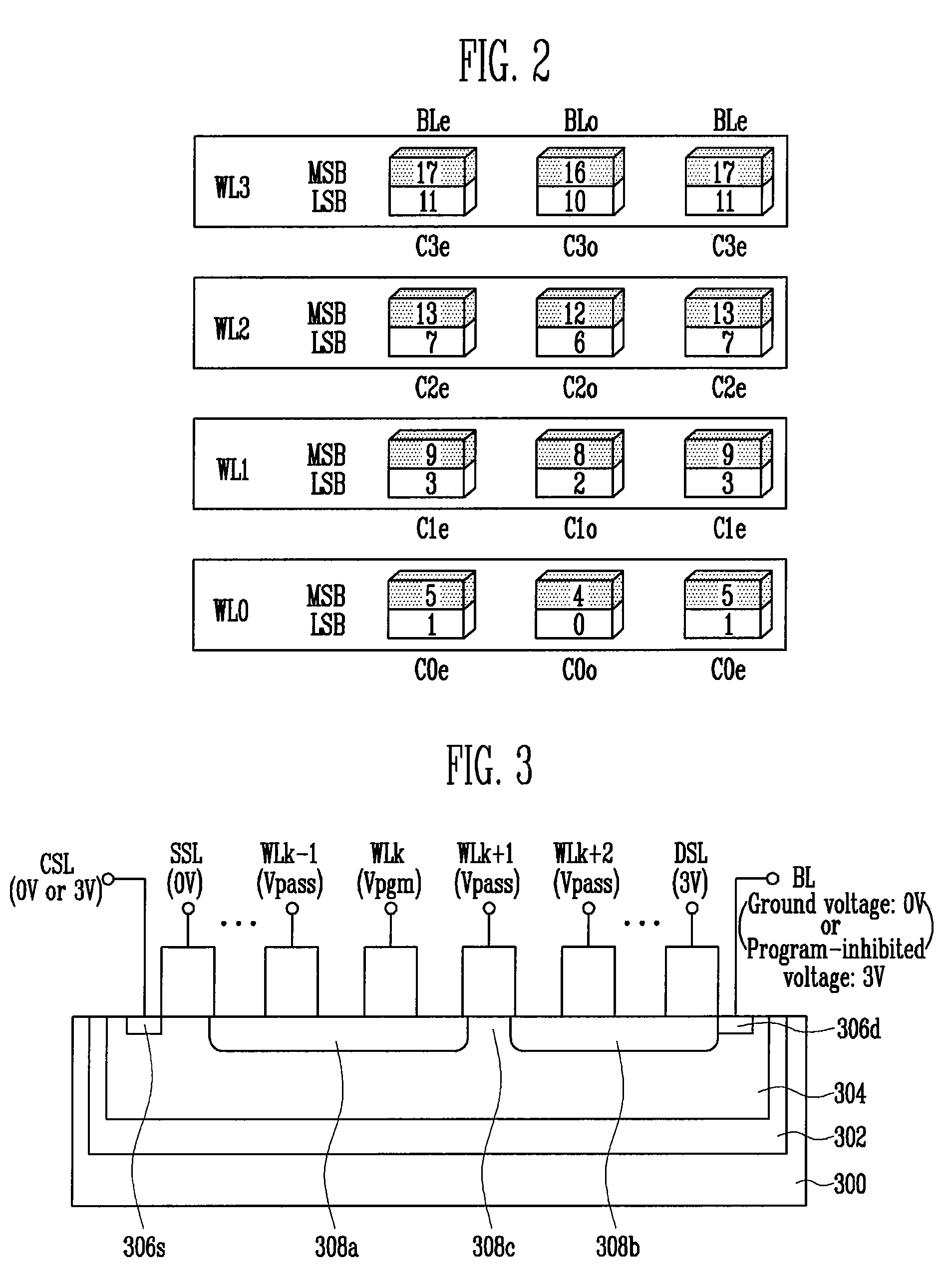
[0036]FIG. 2 is a schematic view illustrating a programming method of a flash memory device according to an embodiment of the present invention. Numbers indicated within the squares designate the sequence of the LSB programming operation and the MSB programming operation.

[0037]Referring to FIG. 2, in the programming method according to an embodiment of the present invention, in order to store 2-bit data in one memory cell, the LSB programming operation and the MSB programming operation are executed at every memory cel...


PUM


Abstract

A memory device comprises a drain select line, a source select line, word lines, and a string connected between a bit line and a common source line. A program-inhibited voltage is applied to the bit line and a first voltage of a positive potential is applied to the drain select line. A second voltage for activating a programmed memory cell is applied to a word line to which the programmed memory cell is connected. A programming operation is performed by applying a program voltage to a selected word line and applying a pass voltage to the unselected word lines.

Description

CROSS-REFERENCES TO RELATED APPLICATIONS[0001]The present application claims priority to Korean patent application number 10-2007-091541, filed on Sep. 10, 2007, which is incorporated by reference in its entirety.BACKGROUND OF THE INVENTION[0002]The present invention relates to a programming method of a flash memory device and, more particularly, to a programming method of a flash memory device, in which 2-bits or more of data are stored in one memory cell.[0003]A flash memory device may be a NOR and a NAND type device. The NAND flash memory device is advantageous because it supports a higher level of integration than that of the NOR flash memory device. A memory cell array of a NAND flash memory device includes a plurality of memory cell blocks. This is described in more detail below.[0004]FIG. 1 is a circuit diagram illustrating a memory cell block of a NAND flash memory device.[0005]Referring to FIG. 1, a memory cell block includes a plurality of cell strings ST. The cell strings...

Claims


Application Information

Patent Timeline
Patent Type & Authority Applications(United States)
IPC IPC(8): G11C11/34
CPCG11C16/10G11C16/0483G11C16/12G11C16/34
Inventor JEON, YOO NAMSHIM, KEON SOO
Owner SK HYNIX INC
Why Eureka
Try Eureka