Lithium niobate optical modulator

a technology of optical modulators and lithium niobate, which is applied in the field of lithium niobate optical modulators, can solve the problems of high impedance, high electrical losses, and high potential of lithium niobate mzi devices, and achieves low driving voltage, high impedance, and low electrical loss.

Inactive Publication Date: 2009-03-12
OCLARO NORTH AMERICA
View PDF5 Cites 11 Cited by
  • Summary
  • Abstract
  • Description
  • Claims
  • Application Information

AI Technical Summary

Benefits of technology

[0007]Lithium niobate MZI devices have the potential for very broadband operation, but they are limited by, inter alia, mismatches between optical and microwave effective refractive indices (and hence mismatches between the velocities of the electrical and optical signals), electrode electrical losses, electrode impedance and drive voltage. Specifically, a velocity mismatch between the velocities of the electrical and optical signals together with electrical losses strongly curb modulator electro-optical response; high electrode impedance is needed to prevent reflections when the modulator is connected to a signal electrical driver; and low driving voltages are a prerequisite. Introducing a very thin dielectric layer between the MZI structure and the electrodes can provide velocity matching between the electrical and optical fields, low electrical losses and high impedances, but requires higher driving voltages. Modulators made accordingly based on both X-cut and Z-cut lithium niobate substrates perform well up to 10 GHz (the electro-optic effect in lithium niobate is anisotropic and highest in the Z direction of the crystal's unit cell; to maximise the electric field in that direction and so the depth of modulation, waveguides in a Z-cut surface will normally be located directly below electrodes, whereas those in an X-cut surface will normally be located in the gap between two electrodes). For operation at frequencies in excess of 10 GHz using the same driving voltage and microwave refractive index values, Z-cut lithium niobate substrates enable lower electrical losses and higher impedances.
[0010]There remains a need for a Z-cut lithium niobate optical modulator design which is capable of operating at frequencies in excess of 10 GHz with matching optical and microwave effective refractive indices, low drive voltage and electrode electrical losses, and high electrode impedance; some forms of the present invention solve this problem, as well as providing choice of chirp values at frequencies at present in use.
[0018]Use of a (second) wide ground electrode in some preferred forms of the invention ensures low electrical loss, while the combination of this with a (first) narrow ground electrode ensures low driving voltage and high impedance. The narrow ground electrode further serves to reduce the microwave effective refractive index relative to the optical refractive index.

Problems solved by technology

Lithium niobate MZI devices have the potential for very broadband operation, but they are limited by, inter alia, mismatches between optical and microwave effective refractive indices (and hence mismatches between the velocities of the electrical and optical signals), electrode electrical losses, electrode impedance and drive voltage.
Such structures provide high impedance, but also high electrical losses.
These structures present problems with electrical-optical signal velocity matching, which may be overcome by use of very thick gold electrodes (>30 μm), though such thicknesses are difficult to obtain using standard processes.
Such structures also cannot achieve very low electrical losses suitable for high frequency applications, and their structure does not permit easy electrical connections to be made within a package.
However, narrow electrodes suffer from very high electrical losses.

Method used


Image

  • Lithium niobate optical modulator
  • Lithium niobate optical modulator
  • Lithium niobate optical modulator

Examples


Embodiment Construction

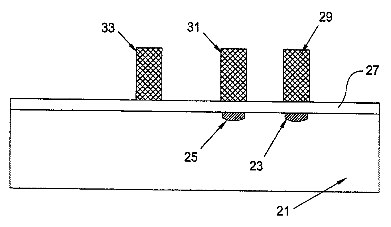
[0027]A first preferred asymmetric coplanar waveguide modulator structure according to the invention, shown in FIGS. 4 and 5, comprises a Z-cut lithium niobate substrate 21 with a thickness of around 500 μm presenting an optical MZI on its surface. The MZI comprises a mid section having two generally parallel waveguides 23, 25 which converge at either end into single input and output waveguides 22, 26. The parallel waveguides are formed in the plane of the surface of the substrate by a standard titanium diffusion process well known to those skilled in the art of modulator design. The axes of the parallel waveguides 23, 25 are 25 μm apart and they have a depth of around 6 μm and a width of around 10 μm A buffer layer 27 of silicon dioxide having a dielectric constant of around 4 and a thickness of 0.65 μm is grown by means of a conventional electron beam evaporation process directly on the surface of the lithium niobate substrate in which the waveguides 23, 25 are formed. Three paral...


PUM

PropertyMeasurementUnit
frequenciesaaaaaaaaaa
thicknessesaaaaaaaaaa
frequenciesaaaaaaaaaa

Abstract

An optical modulator comprises a Z-cut lithium niobate substrate on which is formed a Mach-Zehnder interferometer having two generally parallel waveguides lying beneath a buffer layer of dielectric material. First and second ground electrodes and a hot electrode are disposed on the buffer layer, the first and second ground electrodes being spaced either side of the hot electrode, the hot electrode and the first ground electrode being proximate to at least apart of the respective waveguides. The electrode structure is unsymmetrical in that (a) the hot electrode and the first ground electrode each have a width substantially less than that of the second ground electrode and or (b) the spacing between the first ground and hot electrodes is different from the spacing between the second ground and hot electrodes. whereby a range of chirp values can be obtained. When the spacing between the first ground and hot electrodes is smaller than the spacing between the second ground and hot electrodes, and preferably the hot and first ground electrodes have a width not exceeding 15 .μm, the modulator is capable of operation at frequencies above 10 GHz, possibly up to around 40 GHz.

Description

CROSS-REFERENCE TO RELATED APPLICATIONS[0001]This application is a divisional of co-pending U.S. patent application Ser. No. 10 / 527,607, filed Mar. 11, 2005, which is a 371 application of PCT / EP03 / 10093, filed Sep. 9, 2003, which claims priority to EP 03075716.5, filed Mar. 12, 2003, and EP 02078774.3, filed Sep. 13, 2002, each application is herein incorporated by reference.BACKGROUND OF THE INVENTION[0002]1. Field of the Invention[0003]This invention relates to lithium niobate optical modulators. In particular, the invention relates to lithium niobate optical modulators with electrode structures enabling chirp parameters to be chosen and controlled; some forms of the invention also achieve operation at high frequencies (bit rates) of up to 40 GHz.[0004]2. Background of the Related Art[0005]As the demand for telecommunications services and bandwidth has boomed, the need for, and advantages of, external modulation in fibre-optic transmission systems has been firmly established. Lith...

Claims


Application Information

Patent Timeline
Patent Type & Authority Applications(United States)
IPC IPC(8): G02F1/035G02F1/225
CPCG02F1/035G02F2201/126G02F1/2255
Inventor GILARDI, GIOVANNIMILANESE, PAOLOPENSA, SIMONE
Owner OCLARO NORTH AMERICA
Why Eureka
Try Eureka