Master electrode and method of forming it

a technology of master electrodes and master electrodes, applied in the direction of microstructured devices, electrical equipment, printed circuit manufacture, etc., can solve the problems of exponential dependence of current density, increased etching rate or plating rate, and increased problem of exacerbated problems

Inactive Publication Date: 2009-03-19
REPLISAURUS GROUP
View PDF6 Cites 34 Cited by
  • Summary
  • Abstract
  • Description
  • Claims
  • Application Information

AI Technical Summary

Benefits of technology

[0014]In an embodiment, the pattern layer may comprise at least one area of conducting material arranged in said first surface in portions between said cavities for being in contact with said substrate conducting material during a plating or etching process for increasing the specific conductivity of said substrate conducting material over said areas.

Problems solved by technology

A problem is that the etching rate or plating rate may be higher in the electrochemical cells located closer to the contact area of the seed layer, such as in the perimeter, than in other areas.
This problem is encountered when etching and / or plating is performed on a substrate provided with a seed layer which conducts the current at the substrate.
This problem is exacerbated by the fact that the current density is exponentially dependent on the cell voltage.

Method used


Image

  • Master electrode and method of forming it
  • Master electrode and method of forming it
  • Master electrode and method of forming it

Examples


Embodiment Construction

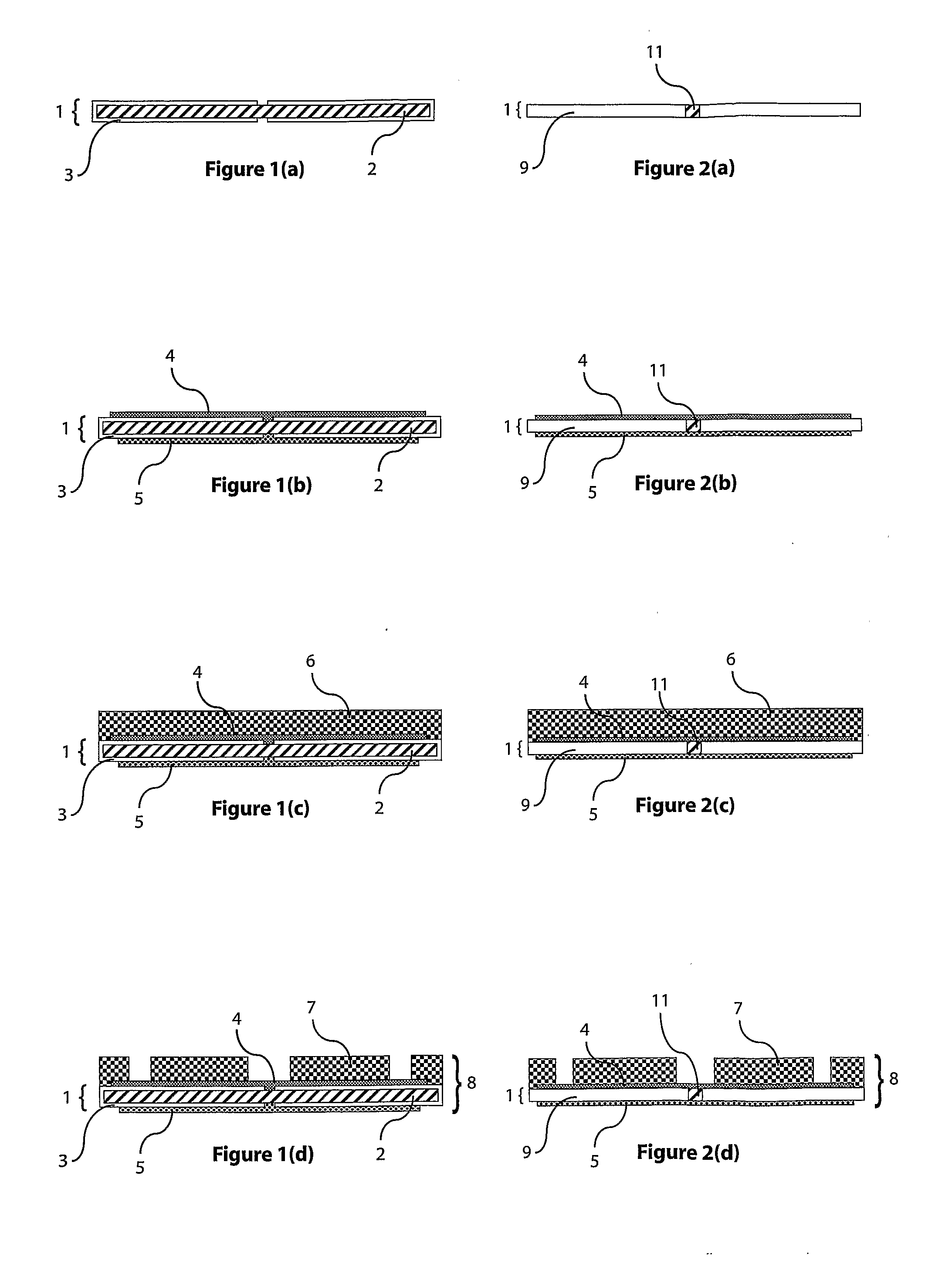
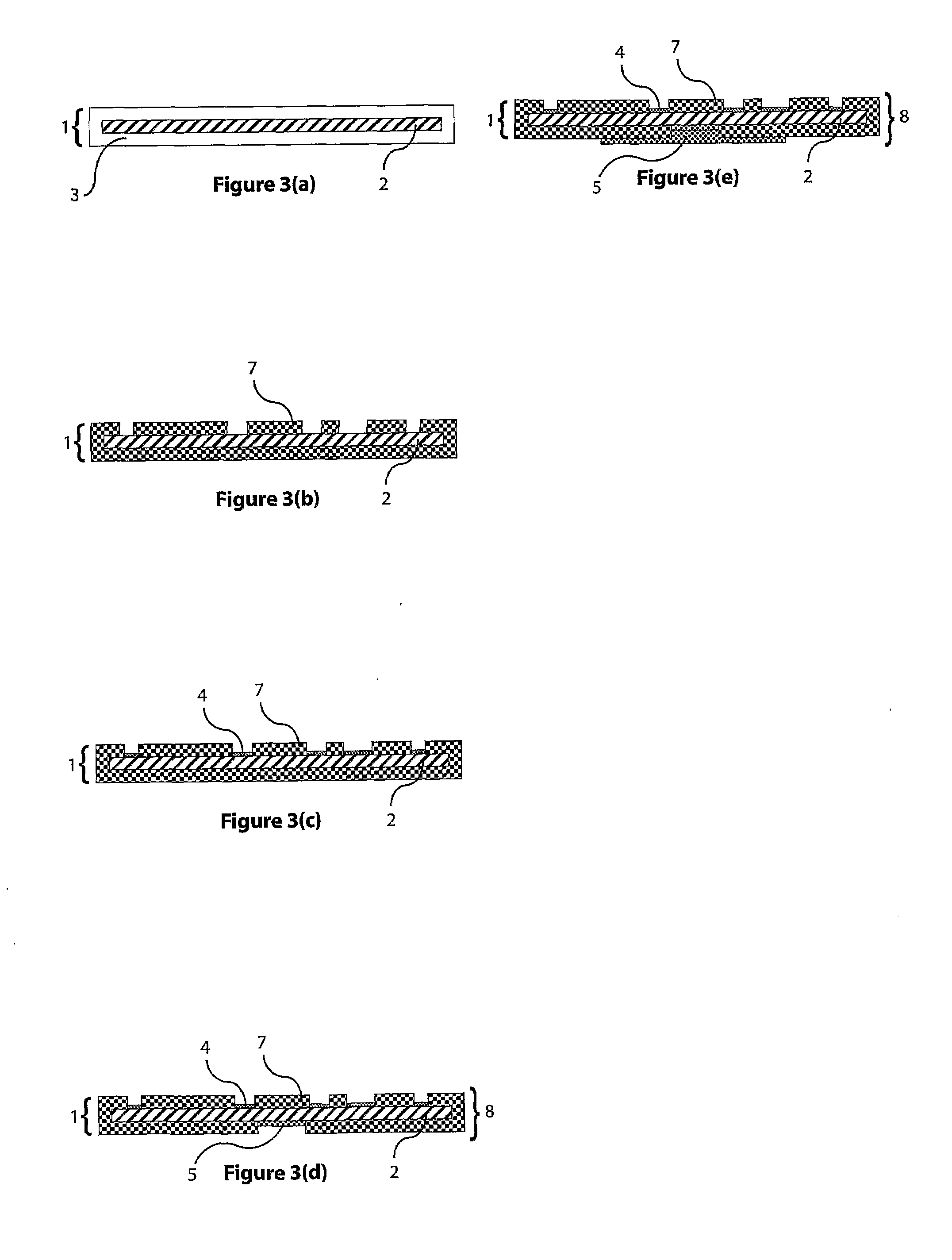
[0046]Below, several embodiments of the invention will be described with references to the drawings. These embodiments are described in illustrating purpose in order to enable a skilled person to carry out the invention and to disclose the best mode. However, such embodiments do not limit the invention, but other combinations of the different features are possible within the scope of the invention.

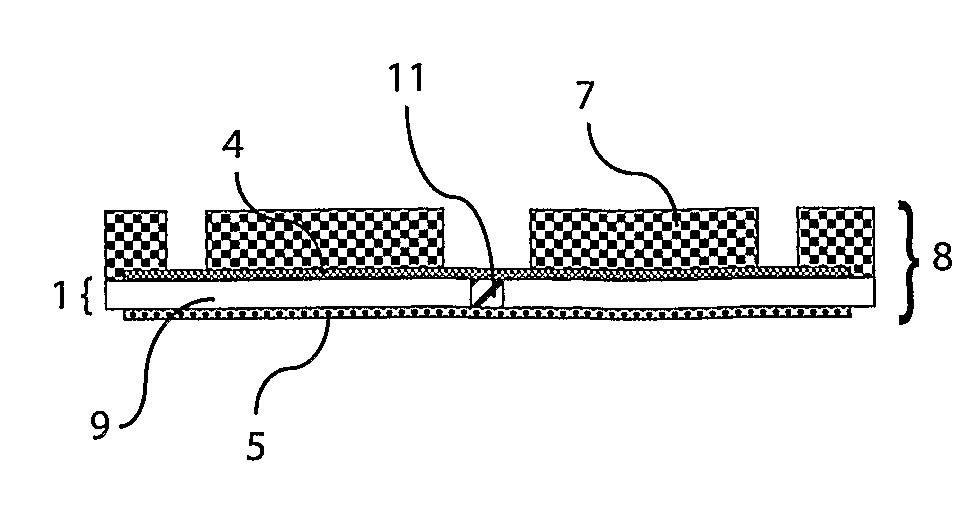
[0047]When etching and / or plating is performed on a substrate provided with a seed layer, which conducts the current at the substrate, it occurs that a substantial potential difference occurs across the seed layer. This being especially true in thin seed layers and at high etching / plating currents. If a potential difference of more than about 1% is present over the electrochemical cells as a result of a potential difference over the surface of the seed layer, the current densities in the electrochemical cells will vary in such an extent that a height difference is observable in the etched / ...


PUM

PropertyMeasurementUnit
thicknessaaaaaaaaaa
current densitiesaaaaaaaaaa

Abstract

A system and method comprising a master electrode arranged on substrate, said master electrode comprising a pattern layer, least partly of an insulating material and having a first surface provided with a plurality of cavities in which a conducting material is arranged, said electrode conducting material being electrically connected to at least one electrode current supply contact; said substrate comprising a top surface in contact with or arranged adjacent said first surface and having conducting material and / or structures of a conducting material arranged thereon, said substrate conducting material being electrically connected to at least one current supply contact; whereby a plurality of electrochemical cells are formed delimited by said cavities, said substrate conducting material and said electrode conducting material, said cells comprising an electrolyte; herein an electrode resistance between said electrode conducting material and said electrode current supply contact and a substrate resistance between said substrate conducting material and said substrate current supply contact are adapted for providing a predetermined current density in each electrochemical cell.

Description

[0001]The present invention relates to a master electrode and a method of forming the master electrode. The master electrode is useable in an etching or plating method as described in a copending Swedish patent application No. 0502538-2 filed Nov. 28, 2005 and entitled “METHOD OF FORMING A MULTILAYER STRUCTURE”. The contents of this specification is incorporated herein by reference. The master electrode is similar to the master electrode described in a copending Swedish Patent Application No. 0502539-2 entitled “ELECTRODE AND METHOD OF FORMING THE ELECTRODE”. The contents of this specification is incorporated herein by reference. The master electrode is suitable for enabling production of applications involving micro and nano structures in single or multiple layers. The master electrode is useful for fabrication of PWB (printed wiring boards), PCB (printed circuit boards), MEMS (micro electro mechanical systems), IC (integrated circuit) interconnects, above IC interconnects, sensors...

Claims


Application Information

Patent Timeline
Patent Type & Authority Applications(United States)
IPC IPC(8): C25D5/02C25D17/00C25D5/00C25F3/02C25C7/02
CPCB81C99/0085Y10T156/10C25F3/14H01L21/2885H01L21/32134H01L21/76838H01L21/76843H01L21/76852H01L21/76873H01L21/76877H01L21/76885H05K3/07H05K3/108H05K3/241H05K3/4647H05K2203/0117H05K2203/0733C23C14/34C23C14/3414C25D5/02C25D5/50C25D7/12C25D1/003C25D5/022C25D7/123C25D5/10C25D7/126C25D1/10
Inventor FREDENBERG, MIKAELMOLLER, PATRIKWIWEN-NILSSON, PETERARONSSON, CECILIADAINESE, MATTEO
Owner REPLISAURUS GROUP
Why Eureka
Try Eureka