
Trench misfet

Inactive Publication Date: 2009-03-19
SHARP KK
View PDF8 Cites 17 Cited by
  • Summary
  • Abstract
  • Description
  • Claims
  • Application Information

AI Technical Summary

Benefits of technology

[0020]An object of the present invention is to realize an improved power MOSFET that reduces an ON resistance per unit cell and enhances a layout effect.
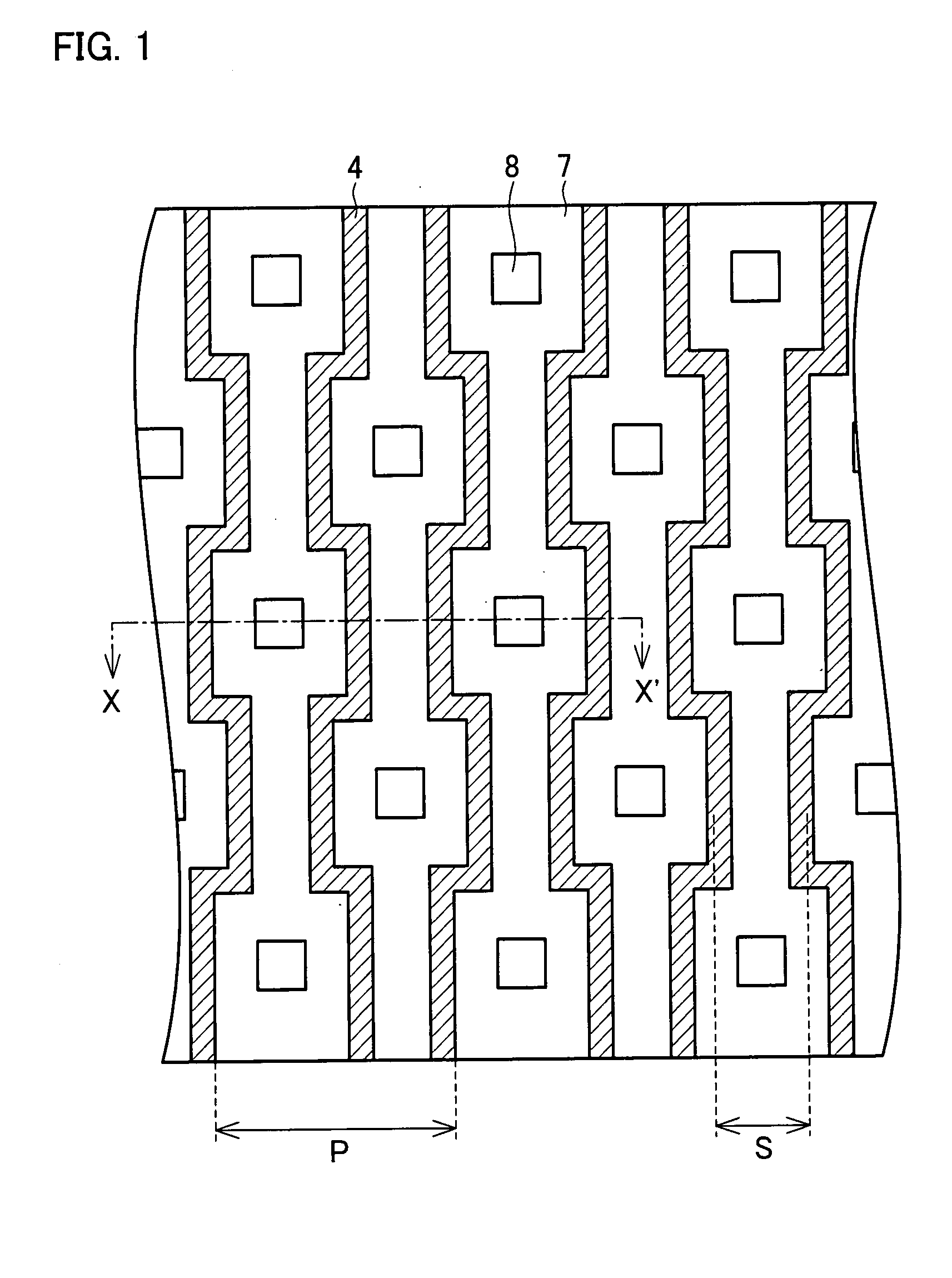
[0023]On the other hand, according to the arrangement mentioned above, a wide region and a narrow region are alternately formed in the regions, including the source diffusion sections and the body diffusion sections, which regions are partitioned by the trench sections. Each of the body diffusion sections is provided in the wide region. This makes it possible, as a whole, to prevent each width between the trench sections from increasing while the body diffusion sections (body contacts) are kept in the arrangement. In other words, the area per unit cell can be suppressed.
[0024]Moreover, for alternate formation of the wide region and the narrow region in the regions including the source diffusion sections and the body diffusion sections, the trench sections are formed to have, for example, a zigzag-shaped part. This increases the length of the periphery of each of the trench sections in a plane, compared with a case where each of the trench sections is formed in a straight line. This leads to an increase in the channel width of the MOSFET.
[0025]Namely, in the trench MOSFET, the pattern layout of the trench sections, the source diffusion sections, and the body diffusion sections as mentioned above leads to an effect such that a cell area is reduced and a channel width is increased. Accordingly, the efficiency of the trench MOSFET can be increased (ON resistance can be reduced).

Problems solved by technology

However, these trench MOSFET techniques of conventional art have following issues (A) and (B).
(B) Conventional cell shapes (hexagon and square shaped types) have a limitation in providing the cells at a fine pitch because the cell shapes require relatively large areas for a body diffusion section (body contact).

Method used


Image

  • Trench misfet
  • Trench misfet
  • Trench misfet

Examples


Embodiment Construction

[0036]Under this heading, a novel trench MISFET (including MOSFET) and its manufacturing method will be described in details according to the present invention. The present embodiment will focus on the present invention being applied to a p-type trench MOSFET. Namely, in the p-type MOSFET in the following explanation, a first conductive type is p-type and a second conductive type is n-type. One with ordinary skill in the art would easily understand that the present invention is applicable not only to p-type trench MOSFETs, but also to n-type trench MOSFETs (where a first conductive type is n-type and a second conductive type is p-type).

[0037]In the trench MOSFET of the present invention, a layout pattern of body contacts and trench sections can be applied to many trench MOSFET variations. The following embodiment is one referential example.

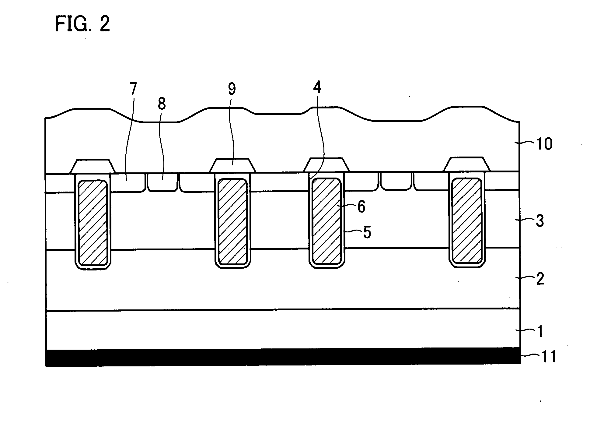
[0038]FIG. 1 illustrates a gate electrode structure and a pattern of contact sections of a source and a body (namely, body contacts) as a basic l...


PUM


Abstract

In one embodiment of the present invention, trench sections cause regions where source diffusion sections and body diffusion sections are formed to be partitioned into line regions. The trench sections are formed not in a straight line shape but in a zigzag shape. Two adjacent trench sections are provided to be axisymmetric, having an axis of symmetry in a longitudinal direction of the trench sections. A wide region and a narrow region are alternately formed in each of the regions, partitioned by the trench sections, in which regions the source diffusion sections and the body diffusion sections are formed. Each of the body diffusion sections is formed in the wide region. This makes it possible to realize an improved power MOSFET that achieves a reduction in an ON resistance per unit cell and an increase in a layout effect.

Description

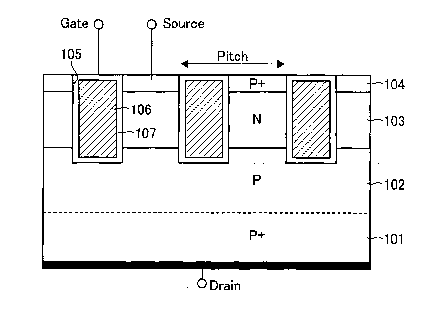
TECHNICAL FIELD[0001]The present invention relates in general to the structure of a semiconductor device and in particular to a trench MISFET (Metal-Insulator-Semiconductor Field Effect Transistor), the trench MISFET having useful applications in power supply devices, for example, DC-DC converters and high-side load drives.BACKGROUND ART[0002]Vertical trench MOSFETs (Metal-Oxide-Semiconductor Field Effect Transistors) have been conventionally used widely in power supply control electronic apparatuses due to their advantages such as their efficient structure and low ON resistance.[0003]FIG. 5 is a cross sectional view illustrating a structure of a conventional, typical n-channel trench MOSFET. (See, for example, Non-Patent Document 1). The n-channel trench MOSFET includes a substrate 101, an epitaxial layer 102, a body section 103, source diffusion sections 104, and body diffusion sections (a pattern of the body diffusion sections (not illustrated in FIG. 5) is formed in the same lay...

Claims


Application Information

Patent Timeline
IPC IPC(8): H01L29/78
CPCH01L29/0696H01L29/7813H01L29/4238
Inventor ADAN, ALBERTO O.
Owner SHARP KK
Learn More