Semiconductor element and device using the same

a technology of semiconductor elements and semiconductor devices, applied in semiconductor devices, instruments, computing, etc., can solve the problems of increasing manufacturing costs, reducing the efficiency of fn tunneling, and high voltage required for write and/or erase (write/erase) operations, etc., to achieve low cost, high reliability, and large memory window

Inactive Publication Date: 2009-03-19
SHARP KK
View PDF3 Cites 9 Cited by
  • Summary
  • Abstract
  • Description
  • Claims
  • Application Information

AI Technical Summary

Benefits of technology

[0014]In view of solving the above problems, the present invention aims to provide at low cost a semiconductor element suited for mass production having a large memory window and having memory characteristics of high reliability by performing high speed write and erase oper

Problems solved by technology

There is thus is a problem in that high voltage is required for the write and/or erase (write/erase) operation.
A power supply or a booster circuit for supplying such high voltage for write/erase thus becomes necessary, which increases the manufacturing cost.
If the write/erase voltage is l

Method used


Image

  • Semiconductor element and device using the same
  • Semiconductor element and device using the same
  • Semiconductor element and device using the same

Examples


first embodiment

[0119]Two states, that is, a write state and an erase state related to information storage are defined as below in the following description.

[0120]The write state is defined mainly as when a majority carriers of carriers in a conductivity type of first and second diffusion layer regions are accumulated in a gate insulating film having a function of accumulating charges. The erase state is defined as when the carriers of the opposite type are mainly accumulated or when the accumulated charges are effectively scarce. The erase state includes a case where the electron holes and the electrons are both accumulated and thus cancel out the respective potentials, so that the accumulated charges are effectively scarce.

[0121]A semiconductor element according to the present invention is a P-channel semiconductor element in which the first and second diffusion layer regions are P-type. In this case, a state in which the electron holes are mainly accumulated in the gate insulating film having a ...

second embodiment

[0215]A second embodiment of the present invention will now be described using FIG. 11.

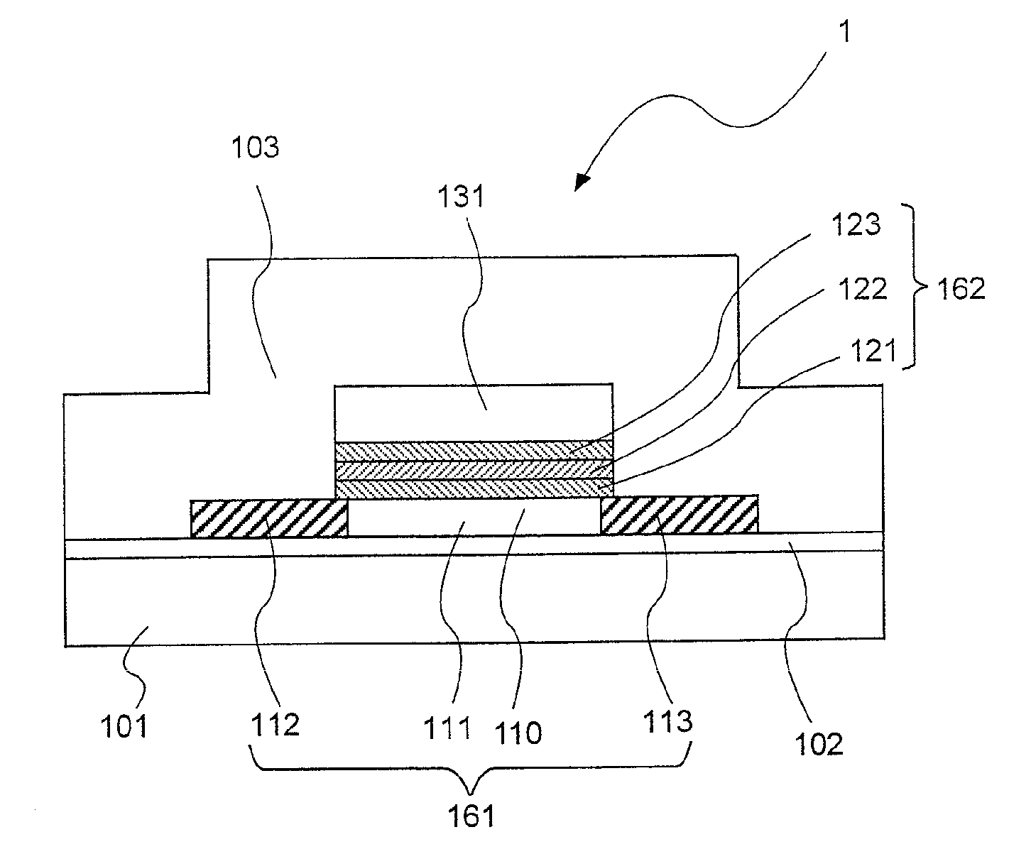
[0216]FIG. 11A is a cross-sectional frame format view taken along line A-B of FIG. 11B, and FIG. 11C is a plan frame format view. Similar, to the first embodiment, the cross-sectional structure has the body region 111 and the P-type diffusion layer regions 112, 113 arranged in the semiconductor layer 161, the surface of the body region 111 between the P-type diffusion layer regions 112 and 113 forming the channel region 110, and the charge accumulating film 162 and the gate electrode 131 existing on the upper part thereof.

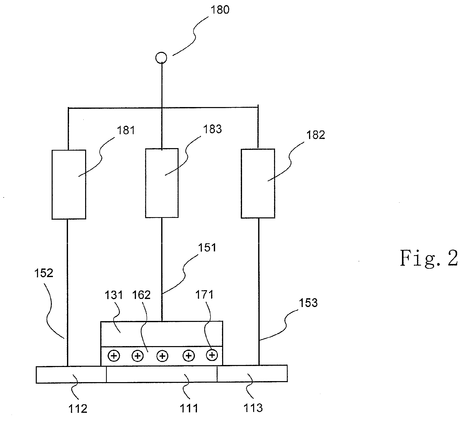
[0217]The second embodiment has a feature in that an electrode terminal (not shown) for controlling the potential of the body region is arranged contacting the body region 111. As a most preferred mode, one example is as shown in FIG. 11B, where one part of the body region 111 is a body contact region 114 having a conductivity-type of N-type, and the electrode terminal (not shown...

third embodiment

[0268]A third embodiment of the present invention uses a memory element shown in first and second embodiments in a liquid crystal display device.

[0269]The liquid crystal display device is configured with the liquid crystals sandwiched between the pair of substrates, scanning lines 512 and signal lines 513 are formed on one substrate as shown in FIG. 25A, and a drive circuit 510 for selectively driving a pixel electrode corresponding to one pixel is arranged, one pixel being a region surrounded by the scanning line 512 and the signal line 513. Each pixel electrode faces the opposite electrode formed on the other substrate with the liquid crystals interposed in between, and selectively drives one pixel.

[0270]The third embodiment has a feature in that the memory element shown in the first embodiment is formed on the panel substrate of the liquid crystal display device. In this case, the memory element of the present invention is used as an element for accumulating image information to ...


PUM


Abstract

A memory element having a large memory window and a high reliability is provided at low cost by performing high speed write and erase operations at a relatively low voltage and suppressing rewrite degradation. A memory element includes a semiconductor layer arranged on an insulating substrate, a first diffusion layer region and a second diffusion layer region having a conductivity type of P-type, a charge accumulating film for covering a channel region between the first diffusion layer region and the second diffusion layer region and being injected with charges from the channel region, and a gate electrode positioned on a side opposite to the channel region with the charge accumulating film in between.

Description

CROSS-REFERENCE TO RELATED APPLICATION[0001]This application is related to Japanese Patent Application No. 2007-241162 filed on Sep. 18, 2007, and Japanese Patent Application No. 2007-241180 filed on Sep. 18, 2007 whose priorities are claimed and the disclosure of which is incorporated by reference in its entirety.BACKGROUND OF THE INVENTION[0002]1. Field of the Invention[0003]The present invention relates to a semiconductor element, a driving method, and a semiconductor device including a drive circuit of the semiconductor element. More specifically, the present invention relates to a semiconductor element for accumulating charges in an insulating body having a level for trapping charges, a driving method, and a device equipped with a drive circuit of the semiconductor element such as display device, liquid crystal display device and receiver.[0004]2. Description of Related Art[0005]A semiconductor memory element is generally formed using a semiconductor substrate. A device using a...

Claims


Application Information

Patent Timeline
IPC IPC(8): G09G5/00H01L29/792G05F1/10
CPCH01L29/792H01L29/66833
Inventor KATAOKA, KOTAROIWATA, HIROSHIOHTA, YOSHIJIKIMOTO, KENJIKOMIYA, KENJIADACHI, KOUICHIROSHIBATA, AKIHIDEHARADA, MASATOMI
Owner SHARP KK
Why Eureka
Try Eureka