Fast Triggering ESD Protection Device and Method for Designing Same

a protection device and fast triggering technology, applied in the direction of emergency protective arrangements for limiting excess voltage/current, instruments, electric digital data processing, etc., can solve the problem of overshoot still appearing over the ic, and achieve the effect of further reducing the overshoot over the i

Inactive Publication Date: 2009-03-19
INTERUNIVERSITAIR MICRO ELECTRONICS CENT (IMEC VZW)
View PDF5 Cites 13 Cited by
  • Summary
  • Abstract
  • Description
  • Claims
  • Application Information

AI Technical Summary

Benefits of technology

[0005]The present embodiments of the invention provide an ESD protection device and method

Problems solved by technology

The prior art has shown that the problem of the overshoot still appe

Method used


Image

  • Fast Triggering ESD Protection Device and Method for Designing Same
  • Fast Triggering ESD Protection Device and Method for Designing Same
  • Fast Triggering ESD Protection Device and Method for Designing Same

Examples


first embodiment

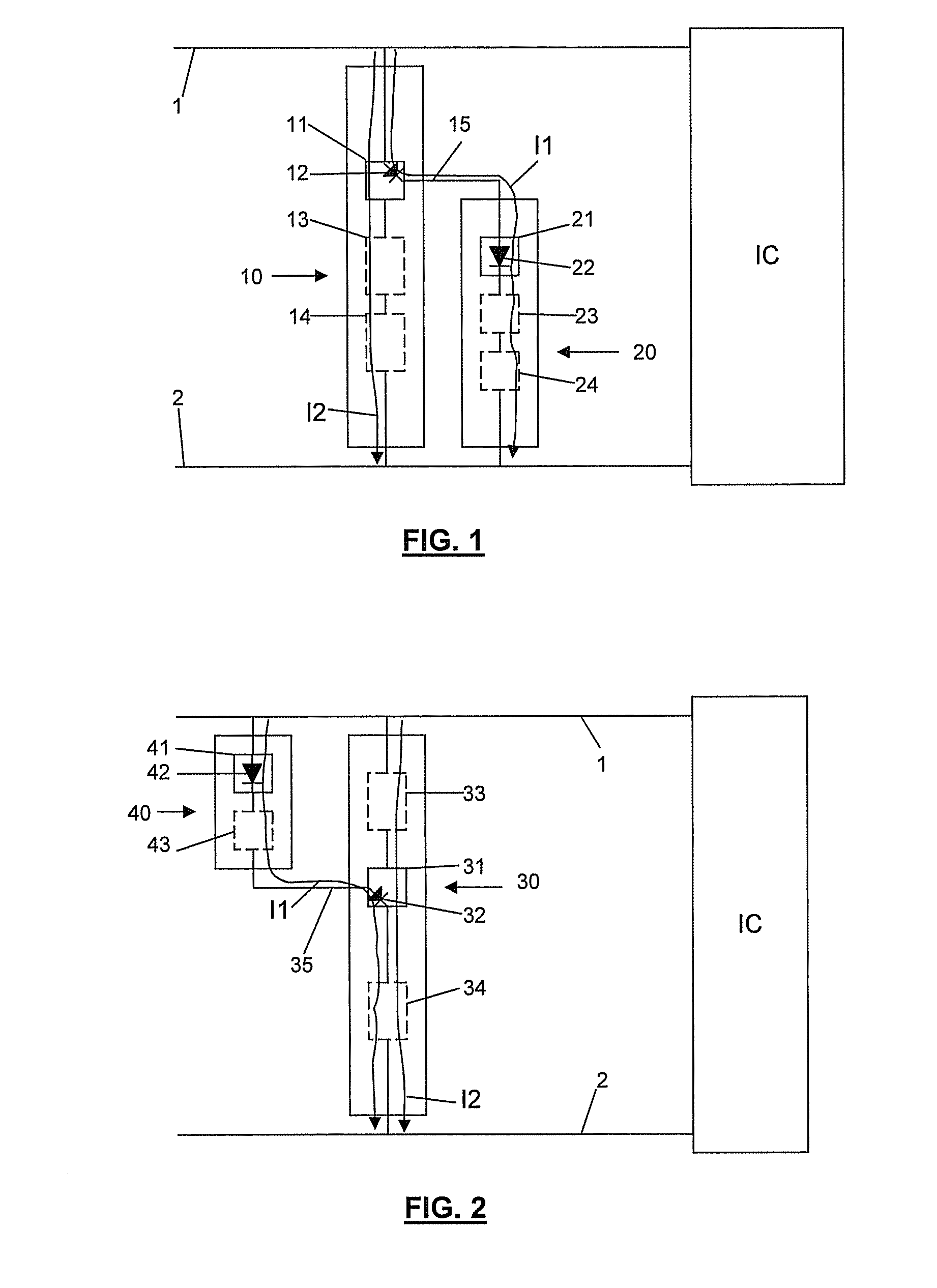
[0037]an ESD protection circuit is shown in FIG. 1. The circuit is designed for protecting an integrated circuit “IC” connected between a first node 1 and a second node 2 against an ESD event. The circuit comprises a main ESD device 10 and a triggering device 20. The main ESD device 10 is connected between the first and second nodes 1, 2 and is arranged for being triggered upon an ESD event and subsequently conducting ESD current from the first node 1 to the second node 2. This current is represented as the arrow I2. The main ESD device comprises a first component 11 with a first diode 12 and possibly other components 13, 14 in the current path I2. The first component 11 forms a triggering node 15 of the main ESD device 10 by means of which the device can be triggered for conducting the current I2. The triggering device 20 is connected between the triggering node 15 of the main ESD device 10 and the second node 2 and is added to reduce the triggering voltage of the main ESD device 1...

second embodiment

[0038]an ESD protection circuit according to the invention is shown in FIG. 2. The circuit comprises a main ESD device 30 and a triggering device 40. The main ESD device 30 is connected between the first and second nodes 1, 2 and is arranged for being triggered upon an ESD event and subsequently conducting ESD current from the first node 1 to the second node 2. This current is represented as the arrow I2. The main ESD device comprises a first component 31 with a first diode 32 and possibly other components 33, 34 in the current path I2. The first component 31 forms a triggering node 35 of the main ESD device 30 by means of which the device can be triggered for conducting the current I2. The triggering device 40 is connected between the triggering node 35 of the main ESD device 30 and the second node 2 and is added to reduce the triggering voltage of the main ESD device 30. This triggering device 40 comprises a triggering component 41 comprising a second diode 42 and possibly a numbe...

third embodiment

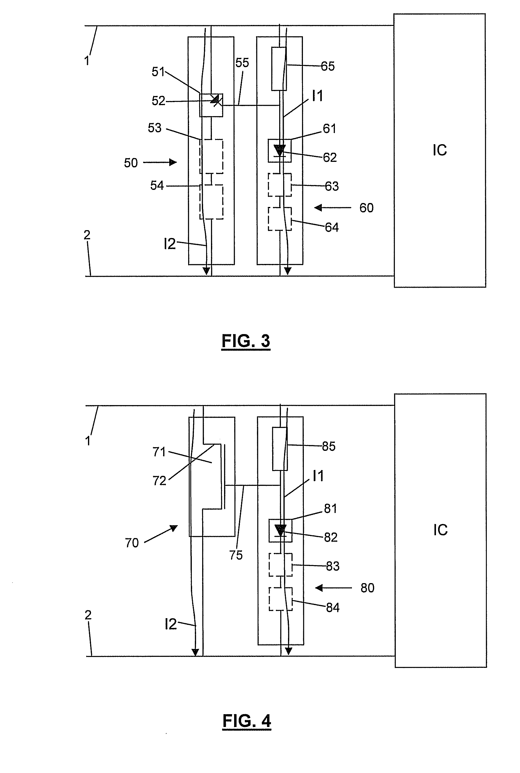
[0039]an ESD protection circuit according to the invention is shown in FIG. 3. The circuit comprises a main ESD device 50 and a triggering device 60. The main ESD device 50 is connected between the first and second nodes 1, 2 and is arranged for being triggered upon an ESD event and subsequently conducting ESD current from the first node 1 to the second node 2. This current is represented as the arrow I2. The main ESD device comprises a first component 51 with a first diode 52 and possibly other components 53, 54 in the current path I2. The first component 51 forms a triggering node 55 of the main ESD device 50 by means of which the device can be triggered for conducting the current I2. The triggering device 60 is connected between the triggering node 55 of the main ESD device 50, the first node 1 and the second node 2. It is added to reduce the triggering voltage of the main ESD device 50. Downstream from the triggering node 55, i.e. between this node and the second node 2, the tri...


PUM


Abstract

A method and apparatus for designing an ESD protection circuit comprising a main ESD device and a triggering device connected to a triggering node of the main ESD device by means of which the main ESD device can be triggered for conducting ESD current at a reduced voltage. The triggering device is located in an initial current path for the ESD current. In this initial current path, there is at least one triggering component which can be triggered from an off-state to an on-state. The triggering speed of this component is considered and its design is optimised in view of increasing its triggering speed. Further shown is an ESD protection circuit in which at least one triggering component is selected to be of a predetermined type for achieving a fast triggering speed, preferably of the gated diode type.

Description

RELATED APPLICATIONS[0001]This application claims priority to European Patent Application No. EP 07116428.9 filed Sep. 14, 2007 which is incorporated herein by reference.FIELD OF THE INVENTION[0002]This invention generally relates to the field of electrostatic discharge (ESD) protection circuitry and, more specifically, improvements for silicon controlled rectifier (SCR) circuits in the protection circuitry of an integrated circuit (IC).BACKGROUND OF THE INVENTION[0003]The ongoing advancements in integrated circuit (IC) technologies have led to the use of lower supply voltages to operate the IC's. Designing IC's with lower supply voltages requires the use of very thin gate oxides. The thickness of the gate oxides influences the amount of drive current that is generated. The thinner the gate oxide layer, the more drive current is generated, which thereby increases the speed of the circuit. The gate oxides (e.g., silicon dioxide) may have a thickness of less than 3 nanometers, and fur...

Claims


Application Information

Patent Timeline
IPC IPC(8): H02H9/00G06F17/50
CPCH01L27/0262H01L29/0649H01L29/7391H03K17/305H01L29/861H03K17/08144H01L29/7436
Inventor THIJS, STEVENTREMOUILLES, DAVID ERIC
Owner INTERUNIVERSITAIR MICRO ELECTRONICS CENT (IMEC VZW)
Why Eureka
Try Eureka