Semiconductor integrated circuit device and method for designing the same

a technology of integrated circuits and semiconductors, applied in the direction of cad circuit design, originals for photomechanical treatment, instruments, etc., can solve the problems of increasing the manufacturing cost of chips, difficult to control patterning accuracy variations to several tens of nanometers, etc., and achieve the effect of reducing the design siz

Inactive Publication Date: 2005-03-22
PANASONIC CORP
View PDF6 Cites 145 Cited by
  • Summary
  • Abstract
  • Description
  • Claims
  • Application Information

AI Technical Summary

Benefits of technology

In accordance with the first method for designing a semiconductor integrated circuit device, the layout design rule is not applied equally to all the plurality of placement regions but the second design rule different from the first design rule is applied to the region (out-of-tolerance region) where the error tolerance for the standard value of the first layout design rule is not satisfied. Since the layout design rule considering even variations in patterning accuracy is not applied equally to all the plurality of placement regions, a design margin can be provided for each of the placement regions, which ensures the miniaturization of the integrated circuit device.
In accordance with the second method for designing a semiconductor integrated circuit device, the layout design rule is not applied equally to all the plurality of placement regions but the second standard value different from the first standard value is applied to the region (out-of-tolerance region) where the error tolerance for the standard value of the first layout design rule is not satisfied. Since the layout design rule considering even variations in patterning accuracy is not applied equally to all the plurality of placement regions, a design margin can be provided for each of the placement regions, which ensures the miniaturization of the integrated circuit device.

Problems solved by technology

As design sizes are reduced increasingly year after year, however, a chip designing process performed by using one layout design rule for one chip encounters the following problems.
In that case, it will become extremely difficult to control variations in patterning accuracy to several tens of nanometers by considering each of variations in patterning accuracy in the fabrication process, which are dependent on the regions (portions) of the principal surface of a wafer, the relationship between the regions (portions) of one chip and layout densities therein, and the like.
As a consequence, the trend toward further miniaturization drastically increases the manufacturing cost for a chip.

Method used


Image

  • Semiconductor integrated circuit device and method for designing the same
  • Semiconductor integrated circuit device and method for designing the same
  • Semiconductor integrated circuit device and method for designing the same

Examples


embodiment 1

Referring to the drawings, EMBODIMENT 1 of the present invention will be described.

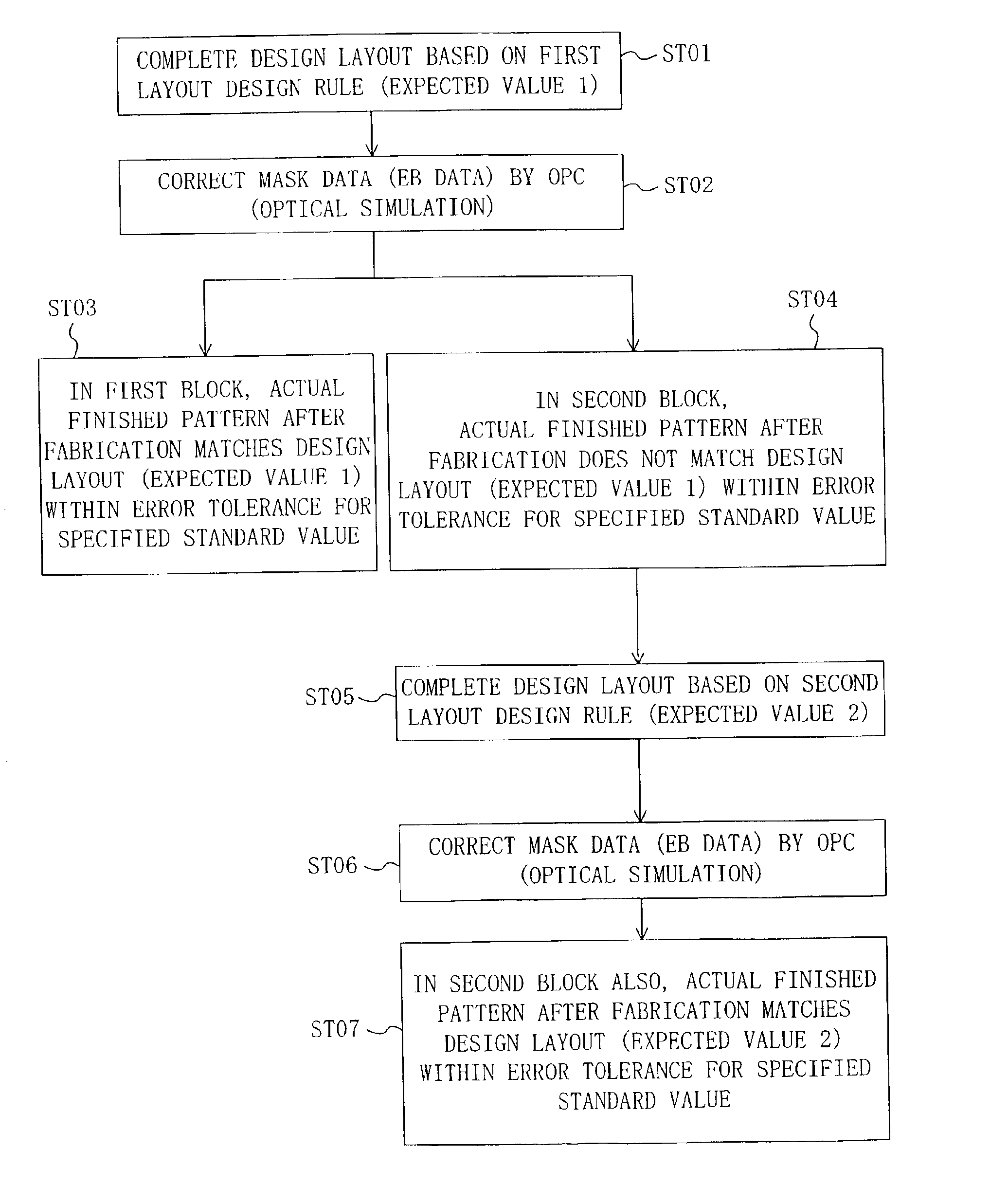
FIG. 1 shows the flow of a method for designing a semiconductor integrated circuit device according to the present invention.

First, in a first-layout-data producing step ST01 shown in FIG. 1, first layout data having a first expected value based on a first design rule is produced for a plurality of placement (layout) regions which are provided on a single semiconductor substrate (chip) and on each of which a design pattern composed of an element pattern and a wiring pattern is to be placed. It is to be noted one placement region does not extend between a plurality of functional blocks.

Next, in a first-OPC-mask-data producing step ST02, the first layout data is optically corrected such that the difference between the first expected value and an expected finished size after fabrication, each of which is based on the first layout data, falls within an error tolerance for a standard value, whereby first O...

example 1 of embodiment 1

A description will be given herein below to the case where “Shorter-Side Direction (gate length) of Quadrilateral” as “Direction”, which is the first geometric feature, is applied to “Relative Design-Rule Sizes” and “Bit Cell Area” which are the first and third categories of the physical dimensions.

FIG. 4A diagrammatically shows a plan structure of a chip-like semiconductor integrated circuit device according to EXAMPLE 1 of EMBODIMENT 1 of the present invention and SRAM blocks formed on the chip. FIG. 4B shows physical dimensions and conditions to be applied to the SRAM blocks.

As shown in FIG. 4A, a first SRAM block 11 having a capacity of 512 kbits, a second SRAM block 12 having a capacity of 128 kbits, and a third SRAM block 13 having a capacity of 16 kbits are formed integrally on a principal surface of a chip 10 composed of, e.g., silicon.

Here, an area (S_bitcell) occupied by a cell corresponding to one bit (bit cell) which composes the first SRAM block 11 is assumed to be 2.4 ...

example 2 of embodiment 1

By way of example, a description will be given herein below to the case where “Layout Density”, which is the second geometric feature, is applied to the determination of “Area of Contacts” or “Number of Contacts” which is the fourth category of the physical dimensions to be applied.

Here, a layout design rule for determining physical dimensions to be applied to “Area of Contact” or “Number of Contacts” is determined selectively based on “Layout Density” which is the second geometric feature.

FIGS. 6A and 6B show a variation of bit cells contained in an SRAM blocks formed in a semiconductor integrated circuit device according to EXAMPLE 2 of EMBODIMENT 1 of the present invention, of which FIG. 6A shows a plan structure of a bit cell provided with two contacts formed in a specified contact formation region and FIG. 6B shows a plan structure of a bit cell provided with one contact formed in a specified contact formation region. In FIGS. 6A and 6B, the description of the same parts of the...


PUM

PropertyMeasurementUnit
areaaaaaaaaaaa
areaaaaaaaaaaa
areaaaaaaaaaaa

Abstract

A method for designing a semiconductor integrated circuit device, the method has the steps of producing, for a plurality of placement regions on each of which a design pattern is to be placed, first layout data having a first expected value based on a first layout design rule, producing, if a difference between the first expected data and an expected finished size after fabrication of the first layout data falls within an error tolerance for a standard value, first OPC data by correcting the first layout data, producing, if the plurality of placement regions include an out-of-tolerance region for which the first OPC data falling within the error tolerance cannot be produced, second layout data having a second expected value for the out-of-tolerance region based on a second layout design rule, producing second OPC data by correcting the second layout data such that an expected finished size after fabrication of the second layout data falls within the error tolerance for the standard value, and producing mask data by using the first OPC data and the second OPC data.

Description

BACKGROUND OF THE INVENTIONThe present invention relates to a semiconductor integrated circuit device which matches the trend toward further miniaturization.As shown in FIG. 27, a conventional method for designing a semiconductor integrated circuit device has produced layout data based on a design rule which is uniform throughout a chip. Layout data is uniquely determined such that the difference between an expected value and a finished physical size after patterning, each of which is based on the layout data, falls within an error tolerance for the expected value.Specifically, if a chip surface includes a region for which first OPC (optical proximity correction) data falling within an error tolerance for a first standard value cannot be produced, second layout data based on a second layout design rule and having a second expected value is redetermined uniquely not only for the region but also for all placement regions, whereby the semiconductor integrated circuit device is redesign...

Claims


Application Information

Patent Timeline
Patent Type & Authority Patents(United States)
IPC IPC(8): G06F17/50G03F1/14G03F1/36G03F1/68G03F1/70H01L21/82H01L21/8244H01L27/10H01L27/11
CPCG06F17/5068G03F1/144G03F1/36G06F30/39
Inventor YAMAUCHI, HIROYUKI
Owner PANASONIC CORP
Why Eureka
Try Eureka