Substrate preparation for thin film solar cell manufacturing

a technology of conductive foil and substrate, which is applied in the manufacture of final products, coatings, basic electric elements, etc., can solve the problems of reducing the efficiency of devices, reducing the adhesion of mo to the substrate, and reducing the effective series resistance of devices.

Inactive Publication Date: 2009-03-26
SOLOPOWER
View PDF7 Cites 34 Cited by
  • Summary
  • Abstract
  • Description
  • Claims
  • Application Information

AI Technical Summary

Benefits of technology

[0007]The structure of a conventional foil-substrate based Group IBIIIAVIA compound photovoltaic cell such as a Cu(In,Ga,Al)(S,Se,Te)2 thin film solar cell is shown in FIG. 1. The device 10 is fabricated on a base 10A which includes a substrate 11 coated with a conductive layer 13. The substrate 11 is a conductive foil or web, such as such as stainless steel. Various metallic foil substrates, such as Cu, Ti, Mo, Ni, Al, stainless steel have previously been identified for CIGS(S) solar cell applications (see for example, B. M. Basol et al., “Status of flexible CIS research at ISET”, NASA Document ID:19950014096, accession No: 95N-20512, available from NASA Center for AeroSpace Information, and B. M. Basol et al., “Modules and flexible cells of CuInSe2”, Proceedings of the 23rd Photovoltaic Specialists Conference, 1993, page 426). The absorber film 12, which comprises a material in the ...

Problems solved by technology

However, the cost of electricity generated using silicon-based solar cells is higher than the cost of electricity generated by the more traditional methods.
One problem associated with the device structure of FIG. 1 is the surface roughness of the foil substrate 11.
When the solar cells are completed by deposition of the transparent layer 14, these poisoned regions cause excessive current leakage reducing the efficiency of the devices.
Alternately, the regions where the contact layer 13 is discontinuous, don't get coated effectively by the absorber film 12, giving rise to pinholes, which are very undesirable defects for solar cell...

Method used


Image

  • Substrate preparation for thin film solar cell manufacturing
  • Substrate preparation for thin film solar cell manufacturing
  • Substrate preparation for thin film solar cell manufacturing

Examples


Embodiment Construction

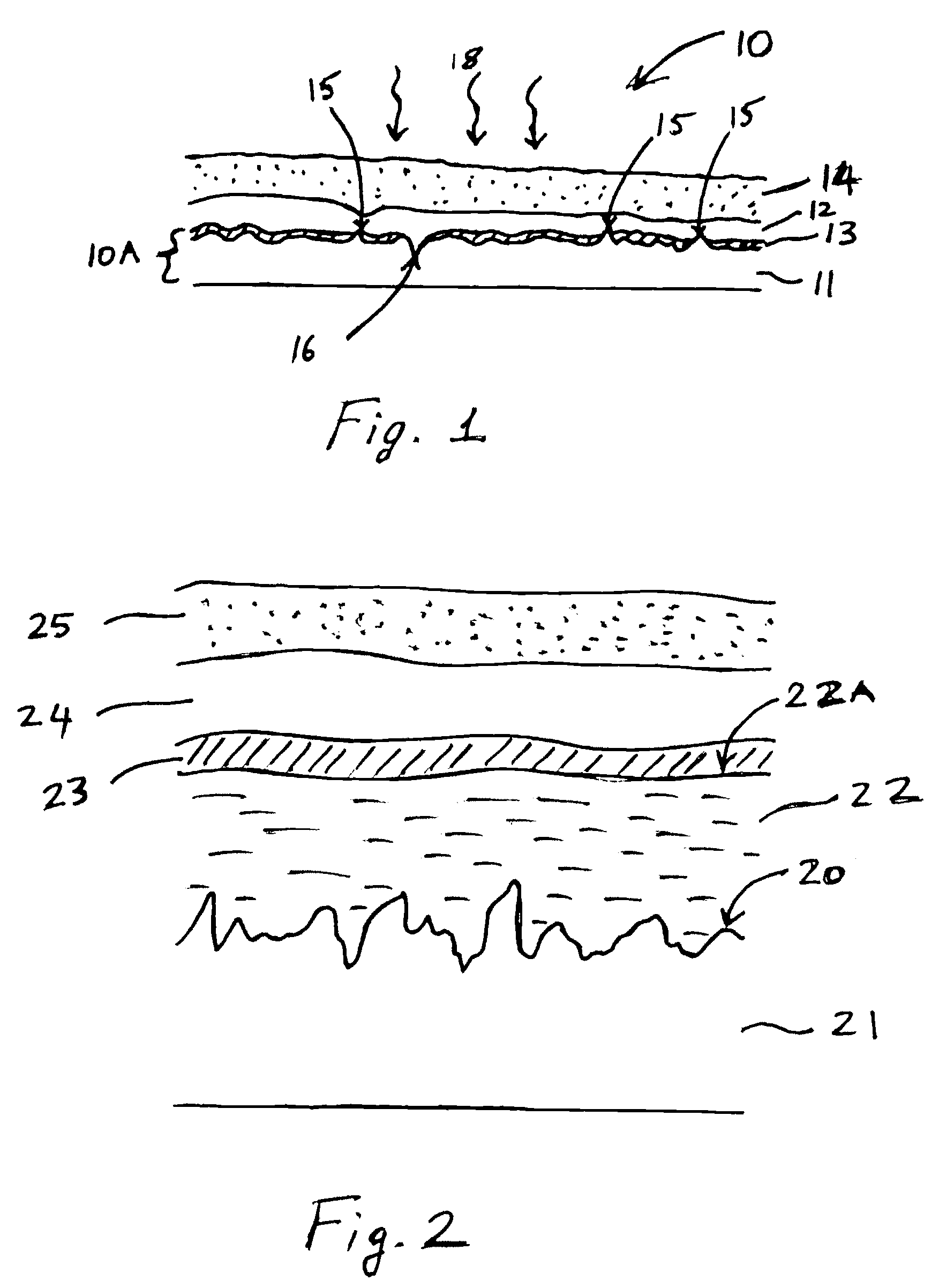
[0018]Embodiments of present inventions provide a flexible foil base that enhances the efficiency and manufacturing yield of flexible II-VI compound semiconductor solar cells, i.e. Group IIBVIA thin film solar cells such as CdTe solar cells and Group IBIIIAVIA thin film solar cells such as CIGS(S) type solar cells. The preferred solar cell structure is a Group IBIIIAVIA thin film solar cell which will be described below.

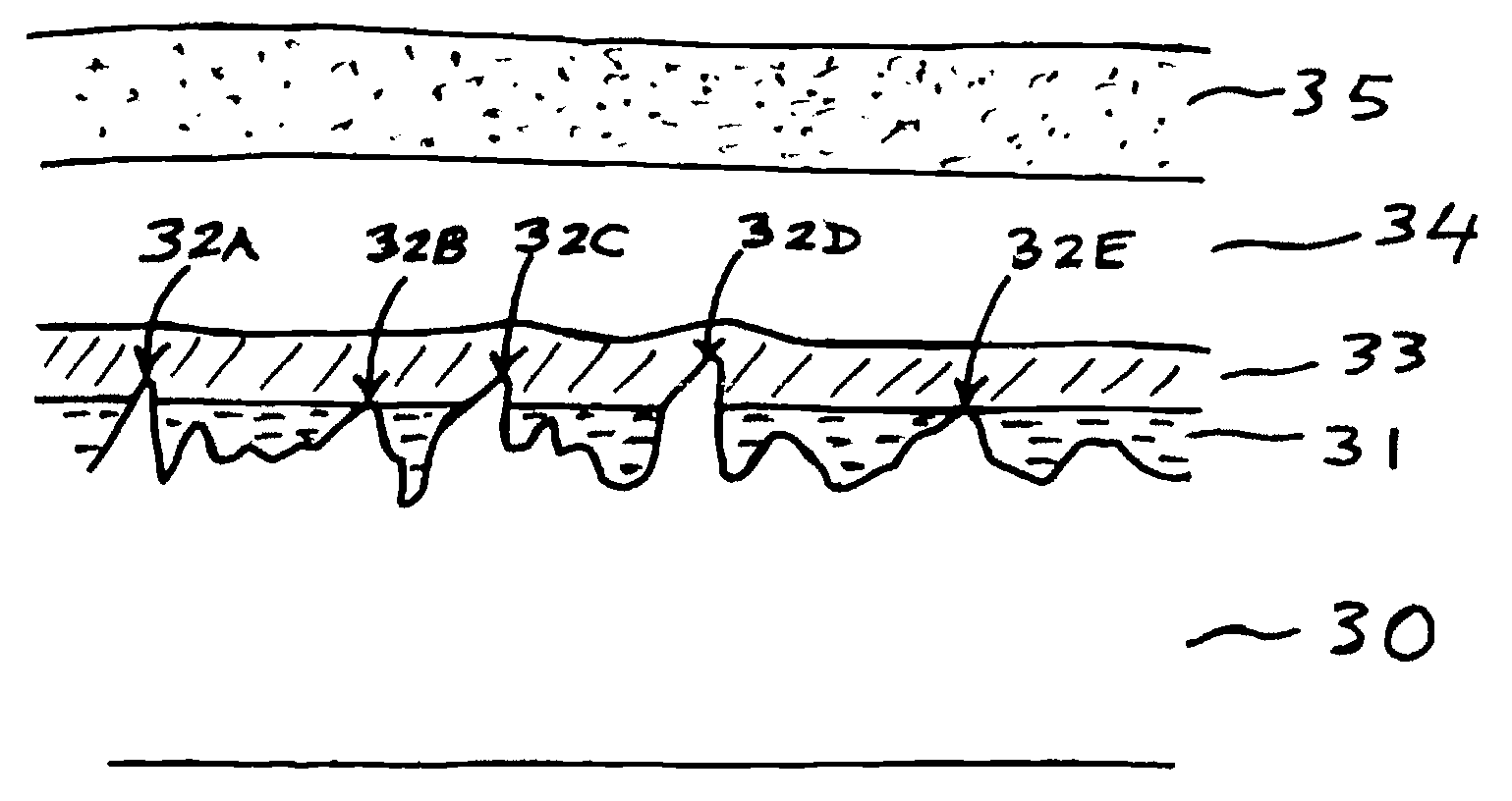
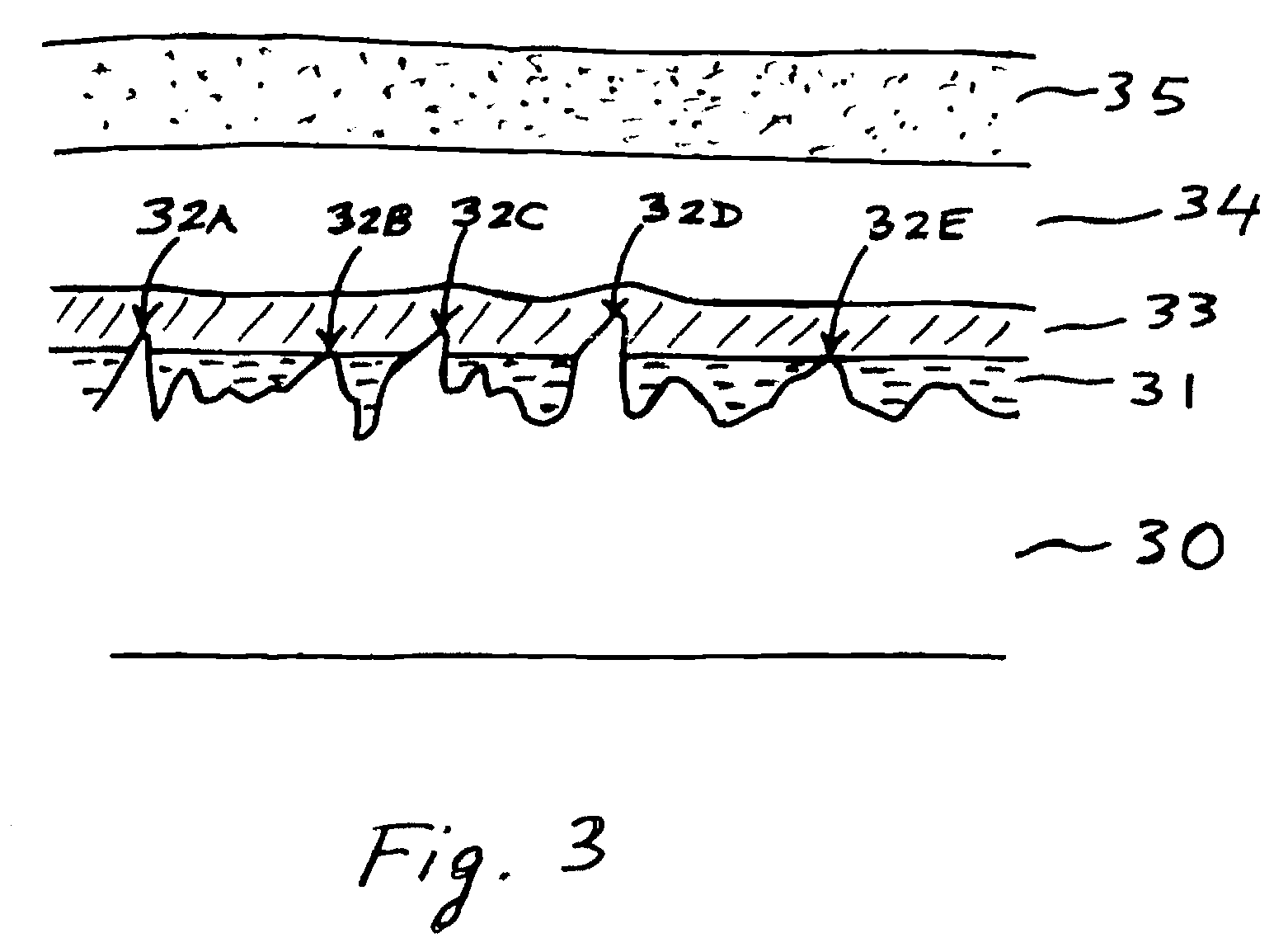
[0019]The base of the thin film solar cell includes a highly conductive metallic substrate that is surface treated using a process that employs an insulating or high resistivity and permanent buffer film to cover the surface of the metallic substrate while the protrusions such as peaks or spikes on the surface are exposed to provide conductivity. Although the embodiments will be described using a CIGS solar cell as an example, it will be appreciated that any flexible thin film solar cell employing a Group IBIIIAVIA compound semiconductor absorber film can be used. In...


PUM

PropertyMeasurementUnit
Temperatureaaaaaaaaaa
Thicknessaaaaaaaaaa
Flexibilityaaaaaaaaaa

Abstract

A thin film solar cell including a Group IBIIIAVIA absorber layer on a defect free base including a stainless steel substrate is provided. The stainless steel substrate of the base is surface treated to reduce the surface roughness such as protrusions that cause shunts. In one embodiment, the surface roughness is reduced by coating surface with a thin silicon dioxide which fills the cavities and recesses around the protrusions and thereby reducing the surface roughness. After the silicon dioxide film is formed, a contact layer is formed over the ruthenium layer and the exposed portions of the substrate to complete the base.

Description

[0001]This application relates to and claims priority from U.S. Provisional Application No. 60 / 973,443, entitled “Substrate Planarization for Thin Film Solar Cell Manufacturing,” filed Sep. 18, 2007, which application is expressly incorporated by reference herein.BACKGROUND[0002]1. Field of the Invention[0003]The present inventions relate to preparation of conductive foil substrates for thin film solar cell fabrication, especially solar cells employing Group IBIIIAVIA absorbers.[0004]2. Description of the Related Art[0005]Solar cells are photovoltaic devices that convert sunlight directly into electrical power. The most common solar cell material is silicon, which is in the form of single or polycrystalline wafers. However, the cost of electricity generated using silicon-based solar cells is higher than the cost of electricity generated by the more traditional methods. Therefore, since early 1970's there has been an effort to reduce cost of solar cells for terrestrial use. One way o...

Claims


Application Information

Patent Timeline
IPC IPC(8): H01L31/00C25D7/12
CPCC25D3/56C25D5/50Y02E10/541H01L31/0322H01L31/03928H01L31/022425Y02P70/50
Inventor BASOL, BULENT M.
Owner SOLOPOWER
Why Eureka
Try Eureka