Adjustable Field Effect Rectifier

Active Publication Date: 2009-03-26
STMICROELECTRONICS INT NV
View PDF103 Cites 26 Cited by
  • Summary
  • Abstract
  • Description
  • Claims
  • Application Information

AI Technical Summary

Benefits of technology

[0014]The present invention comprises an Adjustable Field Effect Rectifier (sometimes “AFER” hereinafter) device having an adjustment pocket or region which permits the device to function reliably and efficiently at high voltages without the negative resistance of prior art devices, while also permitting fast recovery and operation at high frequency without large electromagnetic interference. The process for fabricating a device according to the invention comprises opening the gate oxide followed by ion implantation to create a dopant concentration below that opening. The opening can be covered by oxide, if contact between the doped region and the metal is not desired.
[0015]The introduction of the adjustment pocket of the present invention gives a mu

Problems solved by technology

Oxide on the top is a remnant of the self-alignment process and

Method used


Image

  • Adjustable Field Effect Rectifier
  • Adjustable Field Effect Rectifier
  • Adjustable Field Effect Rectifier

Examples


Embodiment Construction

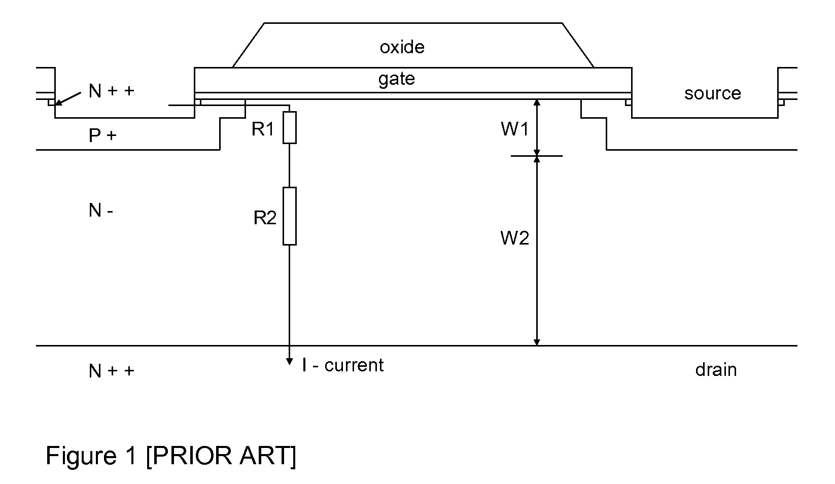
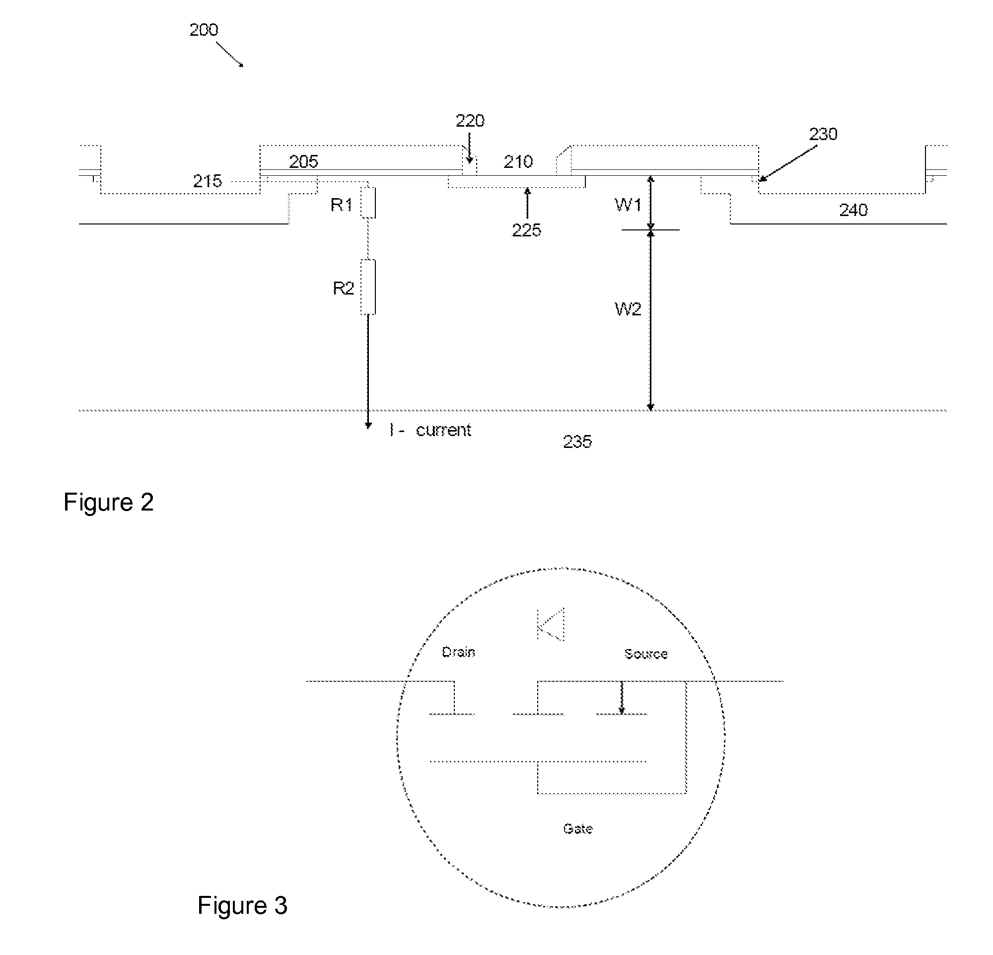
[0033]Referring first to FIG. 2, en embodiment of an Adjustable Field Effect Rectifier (sometimes abbreviated as “AFER” hereinafter for simplicity) in accordance with the invention is shown generally at 200, and in the illustrated arrangement includes an adjustment area, or pocket, discussed in greater detail hereinafter. The barrier for the carrier transport is created under the MOS gate 205 due to the field effect. The barrier height is controlled by the gate material, the gate oxide thickness and the doping concentration in the semiconductor under the gate. A pocket 210 is etched in the middle of the gate, and a shallow P+ implant is created under that opening, which can be insulated from the source 215 via oxide layer 220 or directly connected to the source electrode (for faster performance). The described arrangement is depicted in FIG. 2. For clarity the connection between the source, gate and pocket area is omitted from FIG. 2, but is included in FIG. 4. The connection is typ...


PUM


Abstract

An Adjustable Field Effect Rectifier uses aspects of MOSFET structure together with an adjustment pocket or region to result in a device that functions reliably and efficiently at high voltages without significant negative resistance, while also permitting fast recovery and operation at high frequency without large electromagnetic interference.

Description

RELATED APPLICATIONS[0001]This application claims the benefit of provisional U.S. Patent Application Ser. No. 60 / 975,467, filed Sep. 26, 2007, having the same title as the present application, provisional U.S. Patent Application Ser. No. 60 / 022,968, filed Jan. 1, 2008, entitled “Regenerative Building Block and Diode Bridge Rectifier,” and provisional U.S. Patent Application Ser. No. 61 / 048,336, filed Apr. 28, 2008, entitled “MOSFET with Integrated Field Effect Rectifier,” all of which have the same inventors as the present application and are incorporated herein by reference in full for all purposes.FIELD OF THE INVENTION[0002]The present invention relates generally to rectifiers, and more particularly relates to rectifiers using a Field Effect structure.BACKGROUND OF THE INVENTION[0003]A rectifier is a two terminal device that is commonly used in electric circuits to conduct current in one direction and block current in the opposite direction. The main element of a rectifier is a p...

Claims


Application Information

Patent Timeline
IPC IPC(8): H01L29/68
CPCH01L29/861H01L29/0878H01L29/7802H01L29/41766
Inventor ANKOUDINOV, ALEXEIRODOV, VLADIMIR
Owner STMICROELECTRONICS INT NV
Why Eureka
Try Eureka