Single crystal silicon wafer for insulated gate bipolar transistors and process for producing the same

a technology of insulated gate bipolar transistor and single crystal silicon, which is applied in the field of single crystal silicon wafers, can solve the problems of reducing the pull rate margin within which a defect-free crystal can be grown, lowering production yield, and wafers produced by the cz method are unsuitable for igbt wafers

Active Publication Date: 2009-03-26
SUMCO CORP
View PDF5 Cites 11 Cited by
  • Summary
  • Abstract
  • Description
  • Claims
  • Application Information

AI Technical Summary

Benefits of technology

[0014]Although the above-cited prior alt publications disclose methods for producing crystal defect-free wafers, no mention is made of the wafer characteristics required for IGBTs. Moreover, growing a crystal made of defect-free CZ silicon having an interstitial oxygen concentration of 7×10¹⁷ atoms / cm3 or less and a resistivity variation in the plane of the wafer of 5% or less would require large changes in the rotational speeds of the quartz crucible and the crystal from prior-art conditions, reducing the pull rate margin within which a defect-free crystal can be grown and lowering the production yield.
[0015]It is therefore an object of the present invention to provide methods of manufacturing single crystal silicon wafers for IGBTs that increase the yield and are capable of producing wafers having a small resistivity variation. Another object of the invention is to provide single crystal silicon wafers for the production of IGBTs.

Problems solved by technology

Moreover, growing a crystal made of defect-free CZ silicon having an interstitial oxygen concentration of 7×10¹⁷ atoms / cm3 or less and a resistivity variation in the plane of the wafer of 5% or less would require large changes in the rotational speeds of the quartz crucible and the crystal from prior-art conditions, reducing the pull rate margin within which a defect-free crystal can be grown and lowering the production yield.
However, wafers produced by the CZ method are unsuitable as IGBT wafers for the following reasons.(1) In the CZ method, surplus vacancies agglomerate during single crystal growth, forming crystal originated particles (COP) about 0.2 to 0.3 μm in size.
However, if pits created by the emergence of COPs onto the wafer surface or COPs present near the wafer surface become incorporated into this gate oxide film, the gate oxide integrity will worsen.

Method used


Image

  • Single crystal silicon wafer for insulated gate bipolar transistors and process for producing the same
  • Single crystal silicon wafer for insulated gate bipolar transistors and process for producing the same
  • Single crystal silicon wafer for insulated gate bipolar transistors and process for producing the same

Examples


example 1

Single Crystal Silicon Wafers

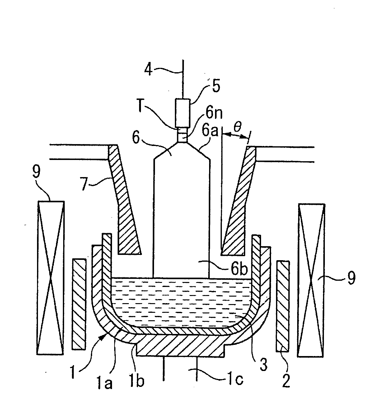
[0113]Silicon ingots having various interstitial oxygen concentrations were produced by the CZ method. Production was carried out by charging a synthetic quartz crucible with 37.5 kg of polysilicon, adding a silicon nitride CVD film-bearing silicon wafer so as to bring the nitrogen concentration in the silicon melt to 2.63×10¹⁷ atoms / cm3, and melting the polysilicon in an argon atmosphere to form a silicon melt.

[0114]Next, a seed crystal was dipped in the silicon melt while applying in a horizontal direction a 0.35 T magnetic field so that the magnetic field center height was positioned 50 mm to the silicon melt side from the liquid surface of the melt, following which the seed crystal was gradually pulled upward while the seed crystal and the synthetic quartz crucible were rotated, thereby growing a single crystal below the seed crystal. Crystal growth was carried out under the following conditions: crucible rate of rotation, 0.05 rpm; crystal rate of r...


PUM


Abstract

A single crystal silicon wafer for use in the production of insulated gate bipolar transistors is made of single crystal silicon grown by the Czochralski method and has a gate oxide with a film thickness of from 50 to 150 nm. The wafer has an interstitial oxygen concentration of at most 7.0×10¹⁷ atoms / cm3, a resistivity variation within the plane of the wafer of at most 5% and, letting tox (cm) be the gate oxide film thickness and S (cm2) be the electrode surface area when determining the TZDB pass ratio, a density d (cm−3) of crystal originated particles (COP) having a size at least twice the gate oxide film thickness which satisfies the formula d≦−ln(0.9) / (S·tox / 2). The wafers have an increased production yield and a small resistivity variation.

Description

[0001]This application is a divisional under 35 U.S.C. §§ 120 and 121 of U.S. patent application Ser. No. 11 / 654,947 filed Jan. 17, 2007 and titled SINGLE CRYSTAL SILICON WAFER FOR INSULATED GATE BIPOLAR TRANSISTORS AND PROCESS FOR PRODUCING THE SAME, which is hereby incorporated by reference for all purposes. Priority under 35 U.S.C. § 119 is claimed to Japanese Patent Application No. 2006-010756, filed Jan. 19, 2006, the content of which is incorporated herein by reference.BACKGROUND OF THE INVENTION[0002]1. Field of the Invention[0003]The present invention relates to single crystal silicon wafers for use in the manufacture of insulated gate bipolar transistors, and to a method of manufacturing such single crystal silicon wafers.[0004]2. Background Art[0005]The insulated gate bipolar transistor (IGBT) is a gate voltage driven switching device suitable for high-power control that is employed, for example, as an inverter in hybrid cars, air conditioning equipment and refrigerators. ...

Claims


Application Information

Patent Timeline
Patent Type & Authority Applications(United States)
IPC IPC(8): H01L21/22
CPCC30B15/04C30B15/305C30B29/06C30B31/20C30B33/04Y10T428/21H01L21/3225H01L29/0657H01L29/66325H01L29/7395H01L21/3221C30B15/20
Inventor UMENO, SHIGERU
Owner SUMCO CORP
Why Eureka
Try Eureka